


Introduction to Rigid Flex PCBs
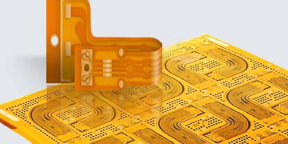
A rigid flex PCB combines rigid and flexible PCB substrates into a single circuit board. The rigid sections provide mechanical support and mounting points, while the flexible sections enable dynamic flexing, bending or folding of the board. Rigid flex PCBs enable more compact and portable device designs by conforming to space constraints and complex geometries. They are commonly used in aerospace, military, consumer electronics, medical devices and automotive applications.
The most common materials used for rigid flex PCB fabrication are:
- Rigid sections: FR-4, CEM-3, polyimide
- Flexible sections: polyimide, polyester, PEEK
Some key benefits of using rigid flex PCB technology:
- Compact, 3D form factor with flexibility
- Component mounting on both sides of flex area
- Eliminates connectors between separate rigid boards
- Improved high frequency performance
- Reduced system weight and costs
- Enhanced reliability with fewer interconnects
Some examples of rigid flex PCB configurations:<table> <thead> <tr> <th>Configuration Type</th> <th>Description </th> </tr> </thead> <tbody> <tr> <td>Flex-rigid</td> <td>Flexible circuitry connecting multiple rigid boards</td> </tr> <tr> <td>Rigid-flex-rigid</td> <td>Rigid boards on both sides of central flex section</td> </tr> <tr> <td>Flex assembled onto rigid</td> <td>Thin flex circuit attached to thicker rigid board</td> </tr> <tr> <td>Rigid assembled onto flex</td> <td>Thin rigid circuit attached to thicker flex board</td> </tr> </tbody> </table>
Rigid Flex PCB Design Considerations
Several important factors must be considered when designing a rigid flex PCB:
Layer Stackup
The rigid and flex sections can have different layer counts based on circuit complexity. However, the flex layer stackup is typically limited to 2-4 layers due to its thinner profile. The rigid layers are normally bonded together through lamination, while the flex layers use adhesive films. The stackup must be optimized to ensure sufficient rigidity, while allowing for flexing without damage.
Substrate Selection
The rigid substrate is commonly FR-4 or a high Tg epoxy, while the flex substrate is polyimide or polyester. The coefficients of thermal expansion between the materials must be matched to prevent warpage and delamination during fabrication and thermal cycling.
Flex-to-Rigid Transition
The junction between the rigid and flex sections requires special attention. The rigid substrate must be gradually tapered to the thinner flex thickness to avoid abrupt transitions that cause stress points. The pad geometries, soldermask definitions and copper pours must also transition smoothly between sections.
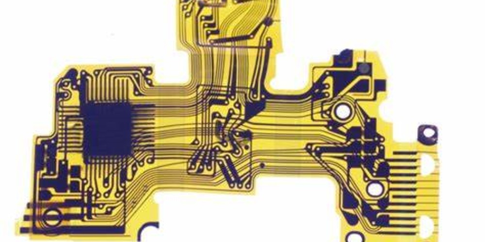
Conductor Layout
Traces should be routed along the centerline of the flex layers, parallel to the bend axis. This reduces stresses from repeated flexing. Minimum trace widths and spacing help increase flexibility. Strategic stiffeners may be added to facilitate and control bending.
Component Placement
Heavier components should be placed on rigid sections, while lighter components can be placed on flex sections. Clearance must be ensured between components on adjacent rigid and flex areas to prevent collisions during flexing.
Vias
To avoid cracking, filled thermal vias are typically used instead of plated through hole vias to connect inner layers across the rigid-flex junction. Microvias also help reduce transition stresses and failures.
Testing
The boards must be subjected to extensive cycle testing to validate the design’s reliability with continuous dynamic flexing without any cracks or electrical malfunctions. This helps identify and correct any potential weaknesses.
Rigid Flex PCB Fabrication Process
Rigid flex PCBs require specialized fabrication capabilities to manufacture the combination rigid-flex structures reliably. Here are the typical production steps:
Layer Preparation
The individual rigid and flex layers are processed separately at first. The rigid layers are laminated together, while the flex layers are bonded using adhesive films. Alignment targets are etched into the layers.
Drilling
The drill and rout tooling must be optimized for the different stock thicknesses. Step-up or zero Z-axis drill technology helps avoid excessive entry burrs.
Lamination
The flex and rigid sub-assemblies are precisely aligned and then laminated together under precise temperature and pressure control. This bonds the sections into an integrated board.
Metalization
The board then goes through metallization to plate the drilled holes and form interlayer connections. This electrically interconnects the rigid and flex sections.
Outer Layer Patterning
The outer layer circuits are etched on both sides of the board to complete the circuit patterning. Solder masks and silkscreens are applied.
Testing and Inspection
Each board is electrically tested. Automated optical inspection and x-ray are used to examine the quality of the rigid-to-flex transitions and layer alignments.
Assembly
Components are soldered using reflow or selective soldering. The boards then undergo functional testing to validate performance.
Guidelines for Assembling Rigid Flex PCBs
Rigid flex PCB assembly requires some specific processes tailored to the unique board construction. Here are some key guidelines:
- Board Handling: Use dedicated nests and carriers designed to secure rigid-flex boards without excessive bending or distortion during transport through assembly steps.
- Solder Paste Stencils: Use laser cut stencils matched to the different rigid and flex areas to ensure precise print definition across varying material thicknesses.
- Component Placement: Place components onto flex areas using pick-and-place heads with specialized vacuum control systems to avoid sucking sections of the thinner board upward.
- Reflow Profile: Use a optimized reflow profile with a controlled heating/cooling ramp that minimizes thermal stresses across the rigid-flex board.
- Inspection: Inspect for proper alignment between rigid and flex sections, sufficient solder fillet sizes in both areas, and any signs of delamination or cracked joints.
- Conformal Coating: Selectively apply acrylic or silicone conformal coating just on the flex areas to prevent corrosion and dendrite growth between conductors.
- Reinforcement: Carefully reinforce component leads and other interfaces between the rigid and flex sections using adhesive or encapsulation.
- Thermal Management: Provide sufficient heat sinking from high power components on rigid sections to prevent localized overheating of adjacent flex areas.
Adhering to these guidelines helps overcome the unique challenges of assembling rigid-flex designs and ensures reliable, high-quality finished boards.
Common Applications of Rigid Flex PCBs
Rigid flex PCBs enable solutions not achievable with rigid boards alone across many industries:
Aerospace and Defense
- Guided missile control surfaces
- RADAR and electronic warfare systems
- Engine control units
- Avionics equipment
Consumer Electronics
- Cell phones, laptops, tablets
- Wearable devices
- Digital cameras
Medical
- Hearing aids
- Implantable devices
- CT scan equipment
- Endoscopes
Automotive
- Powertrain systems
- LED lighting
- Infotainment modules
- Collision detection systems
The unique 3D layout abilities, dynamic flexing capacity and miniaturization offered by rigid-flex makes it the technology of choice for advanced, high reliability products where robustness, size and weight are critical. The applications leveraging rigid-flex circuits are rapidly expanding as technology capabilities improve.
Benefits and Challenges of Rigid Flex PCBs
Benefits
- Ultra-compact, 3D geometries
- Eliminates connectors and harnesses
- Reduced system weight and size
- Improved high speed performance
- Greater reliability with fewer interconnects
- Increased product miniaturization
- Design flexibility and ability to conform to complex shapes
- Cost effective at high volumes
Challenges
- Narrow process margins and tolerances
- Requires advanced expertise to design and build
- Specialized tooling needed for fabrication
- Difficult to modify and repair
- Longer development timelines
- Heightened testing requirements
- Limited number of qualified suppliers
FAQ
What is the typical thickness of the rigid sections in a rigid flex PCB?
The rigid sections typically range from about 0.4 mm to over 2 mm in thickness. Common rigid materials used include 0.8mm, 1.0mm and 1.6mm FR-4 substrates.
How many flex layers can be incorporated in a rigid flex design?
A rigid flex PCB can include from one to four flex layers in most cases. The total flex layer count is limited by the minimum bend radius required. As the number of layers increases, the flex region gets thicker and loses flexibility.
What are some best practices for routing traces in the rigid sections?
Use 45/90 degree angles, avoid acute angles, and minimize the number of vias. Maintain at least 100um spacing between traces for 10Gbps signals, and 250um for speeds over 10Gbps. Minimize length mismatches between differential pairs.
What is the minimum bend radius allowed for the flex layers?
The minimum bend radius is determined by the flex material and stackup. Typical minimum bend radius ranges from 2-3 mm for 1-layer polyimide flex, up to 15 mm for 4-layer polyimide constructions. Flex areas should be designed for at least 150% of the minimum target radius.
What are some methods used to reliably interconnect the rigid and flex sections?
Filled castellated laser drilled (CLD) vias, stacked microvias, filled blind vias and conformal masks are common ways to transition signals between the rigid and flex layers while minimizing stresses.
What testing should be performed to qualify a new rigid flex design?
Prototypes should go through shock/vibration and thermal cycling to verify robustness. The flex areas in particular need dynamic bend life testing, with 180 degree flexing for at least several thousand cycles to validate the design. Electrical continuity should be monitored throughout.