

Flex PCBs, also known as flex circuits or flex PCBs, offer a versatile way to design and integrate electronics into products with space, mobility and reliability constraints. Flex PCBs offer flexibility while maintaining the integrated circuit density and performance of rigid PCBs. With Altium’s robust flex PCB design tools, engineers can seamlessly design rigid-flex PCBs optimized for reliability and cost-effectiveness. This comprehensive guide covers everything needed to get started with and master flex PCB design in Altium.
What are Flex PCBs?
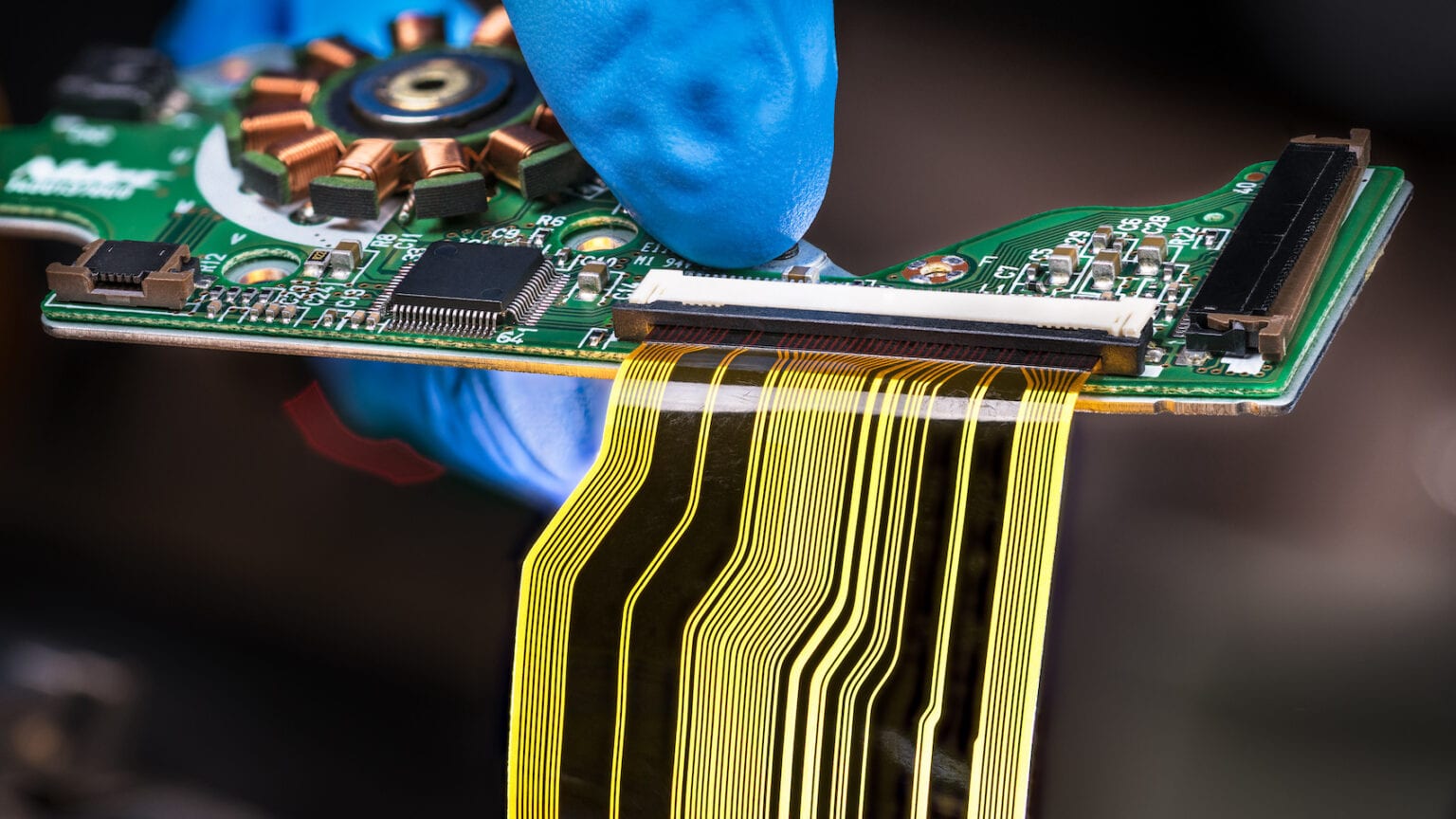
A flex PCB uses a flexible substrate material such as polyimide instead of the more rigid fiberglass used in traditional PCBs. This allows the flex PCB to bend and flex during use. Components are mounted on flexible pads and traces are etched from conductive copper foil onto the polyimide base layer. The flexible material allows the PCB to bend and move within the product’s housing.
Flex PCBs provide several key advantages:
- Reduced space requirements – Flex circuits can fit into tight, constrained spaces where rigid PCBs won’t go. They can fold around other components.
- Flexibility and motion – Products with moving parts like hinges can integrate flex PCBs to maintain connections and circuitry across moving joints.
- Improved reliability – Flex PCBs undergo more motion cycles before failure compared to solder joints from connectors.
- Reduced weight – With a thin, lightweight polyimide substrate, flex PCBs weight much less than glass fiber based rigid-flex PCBs.
Some common applications of flex PCBs include:
- Consumer electronics – Cell phones, cameras, wearables
- Automotive – Sensors, embedded control panels
- Medical – Hearing aids, patient monitoring devices
- Industrial – Robotics, machine controls
Rigid-Flex PCBs
While pure flex PCBs provide the advantages above, some applications require the rigidity and multilayer capabilities of traditional PCBs combined with flex. Rigid-flex PCBs integrate both rigid fiberglass PCB sections and flexible polyimide sections together into one PCB assembly.
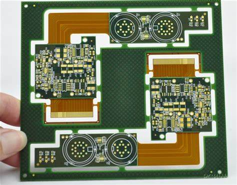
Rigid-flex PCB integrating multiple rigid and flex sections
Rigid sections provide:
- Structural support and component mounting
- Multilayer and high density circuits
- Stiff connectors and ports
While flexible sections allow:
- Bends and flexing motion
- Mechanically decouple rigid sections
Some examples of rigid-flex PCB applications:
- Laptop and mobile device motherboards
- Disk drive flex interconnects
- Automotive camera modules
With rigid-flex PCBs, the rigid and flex sections are photolithographically manufactured together as one integrated board. This eliminates connectors between sections and enhances reliability.
Benefits of Using Altium for Flex PCB Design
Altium Designer provides a complete design environment and set of tools specifically for flex and rigid-flex PCB design. Here are some of the key benefits Altium offers:
- Unified design environment – Rigid and flex sections are designed in the same workspace for seamless rigid-flex design.
- Specialized layer stack manager – Easily define separate layer stacks with different materials for rigid and flex sections.
- Flex and rigid routing – The router handles route paths between layer transitions and bends.
- Flex modeling – Model mechanical stiffness, test clearances with folding simulations.
- Manufacturer validation – Automated DFM checks ensure manufacturability by your fabricator.
- 3D PCB visualization – Instantly visualize a 3D view of your flex or rigid-flex PCB design.
With Altium’s advanced rigid-flex design capabilities, engineers can create compact, reliable electronics and prototypes faster and more cost-effectively.
Design Considerations for Flex PCBs
Designing a successful flex PCB requires considering several key mechanical, electrical, and manufacturing factors:
Mechanical Properties
The thin flexible material must withstand continual bending and flexing during use. Attention must be paid to:
- Minimum bend radius – Below a certain radius, repeated bending will crack the conductive copper traces.
- Flexing endurance – The flex life rating defines the minimum bend radius and number of flex cycles before failure.
- Stiffeners – Rigid sections or stiffening materials may need added to prevent overflexing.
Altium Tools:
- Bend radius rule checks
- 3D bend simulations
- Mechanical layer for stiffeners
Electrical Design
Electrical connections require care on flex PCBs:
- Trace widths and spacing – Thicker traces reduce resistance for handling currents. Narrow spacing allows high circuit density.
- Layer stackup – Additional layers may be needed to route signals across bends.
- Component placement – Ensure components are in suitable locations and orientations for routing.
Altium Tools:
- Flex layer stack manager
- High-speed routing features
- 3D clearance checking
Manufacturing Factors
Work closely with your manufacturer to ensure your design aligns with their process capabilities:
- Flex materials – Match material thickness, flex rating, and copper weights.
- Minimum features – Trace/space capability, annular rings, via spans.
- Handling – Additional stiffeners may be required for manufacturing.
- DFM validation – Run automated checks on manufacturability.
Altium Tools:
- Real-time DFM checks
- Rigid-flex design rule checks
- Fabricator validation queries
Step-by-Step Flex PCB Design Methodology in Altium
Following is an overview of the typical workflow when designing a new flex or rigid-flex PCB in Altium Designer:
1. Initial Planning
- Gather design requirements, constraints, and usage conditions.
- Determine rigid and flex sections.
- Select initial materials, layer stackup, and trace dimensions based on manufacturer’s capabilities.
2. Create New Rigid-Flex Project
- Open a new project and select the target PCB technology: Flexible or Rigid-Flex.
- This preconfigures layers and design rules.
3. Define Layer Stackup
- Use the Stackup Manager to define the layer stack and materials in each section.
- Add cover layers, bond layers, and define copper weights.
4. Design Schematics
- Create schematics and link to PCB with Design > Update PCB.
- Include connectors, ports, and any support hardware.
5. Import Changes to PCB
- Component changes from schematics will import into the PCB.
- Update component footprints if needed.
6. Route and Optimize PCB
- Use Route > Interactive Routing to connect traces.
- Tuning settings can help with clearances, length matching, etc.
7. Analyze Rigid-Flex Performance
- Run Tools > 3D Model to inspect mechanical clearances.
- Use Tools > Bend Points to see flex section folding.
- Validate electrical performance with signal integrity analysis.
8. Generate Manufacturing Outputs
- Run validation checks for DFM errors.
- Generate manufacturing files like Gerbers, drill data.
- Include any mechanical notes for fabrication.
With an iterative design approach utilizing Altium’s built-in tools at each stage, engineers can be highly confident in meeting design requirements and manufacturability.
5 Key Questions and Answers on Altium Flex PCB Design
Here are answers to some frequently asked questions on designing flex PCBs with Altium:
Q1: How is designing a flex PCB different from a rigid PCB?
The core differences are:
- Unique layer stack with flexible substrate
- Attention to mechanical properties like bend radius
- Accommodating motion and flex in traces
- Patterning rigid sections for component mounting
Q2: What are some best practices for routing flex PCBs?
Best routing practices include:
- Minimize trace lengths running across bends
- Use thicker traces for better flex life and current handling
- Include teardrops at pad junctions for reduced stress
- Allow extra spacing around zones crossing bends
Q3: What analysis tools help assess flex PCB reliability?
Key analysis tools include:
- Bend radius rule checks during routing
- 3D modeling of flexed states
- Folding simulations to spot collisions
- Thermal analysis of conductors and vias
- Signal integrity analysis of transmission lines
Q4: How can I check manufacturability of my flex PCB design?
Altium includes real-time DFM checks that validate:
- Minimum clearance requirements
- Trace widths and spacing
- Pad shapes and drill sizes
- Annular rings, acute angles
- Materials and finished layer definitions
Staying within your flex PCB manufacturer’s capabilities is essential.
Q5: What fabrication documentation does my manufacturer need?
Typical documentation includes:
- Layer plots detailing stackup
- ODB++ manufacturing files
- Gerber files of each layer
- Drill and milling files
- 2D drawings with callouts
- 3D step models
- Readme notes on any special instructions
Conclusion
Flex PCBs provide rugged and space-efficient solutions for integrating circuits and components in tight spaces under motion. Rigid-flex PCBs incorporate both flex sections for flexure and folding along with rigid sections for mounting components and traces. Altium Designer offers advanced and dedicated tools for flex and rigid-flex PCBs that simplify designing for mechanical reliability and manufacturability. Engineers can have full confidence implementing flex PCBs in products from inception through fabrication and assembly by following Altium’s streamlined design methodology.