


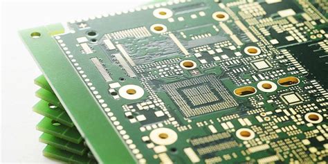
Introduction to Ceramic PCB
Ceramic printed circuit boards (PCBs) are a type of substrate material used in the manufacturing of electronic circuits. Unlike traditional PCBs that use organic materials like FR-4, ceramic PCBs are made from inorganic materials such as alumina (Al2O3) or aluminum nitride (AlN). These materials offer unique properties that make ceramic PCBs suitable for high-performance applications in various industries, including aerospace, automotive, and telecommunications.
Advantages of Ceramic PCBs
Ceramic PCBs offer several advantages over traditional organic PCBs:
- High thermal conductivity: Ceramic materials have excellent thermal conductivity, allowing for better heat dissipation and improved thermal management in electronic circuits.
- Low dielectric constant: The low dielectric constant of ceramic materials reduces signal loss and improves signal integrity, making ceramic PCBs ideal for high-frequency applications.
- High mechanical strength: Ceramic PCBs are more rigid and durable than organic PCBs, offering better resistance to vibration, shock, and thermal stress.
- Excellent dimensional stability: Ceramic materials maintain their shape and size under varying environmental conditions, ensuring consistent performance and reliability.
Applications of Ceramic PCBs
Ceramic PCBs are used in various applications that require high performance, reliability, and durability:
- Aerospace and defense: Ceramic PCBs are used in satellite communication systems, radar systems, and Military Electronics due to their ability to withstand extreme temperatures and harsh environments.
- Automotive: In the automotive industry, ceramic PCBs are used in engine control units, power electronics, and sensor systems, where they provide reliable performance under high temperatures and vibrations.
- Telecommunications: Ceramic PCBs are used in high-frequency applications such as 5G networks, microwave devices, and radio frequency (RF) circuits, where low signal loss and high signal integrity are critical.
- Medical devices: Ceramic PCBs are used in medical equipment such as implantable devices, surgical instruments, and diagnostic tools, where they offer high reliability and biocompatibility.
Manufacturing Process of Ceramic PCBs
The manufacturing process of ceramic PCBs differs from that of traditional organic PCBs. The process involves several steps, including:
1. Raw Material Preparation
The first step in manufacturing ceramic PCBs is preparing the raw materials. The most commonly used ceramic materials are alumina (Al2O3) and aluminum nitride (AlN). These materials are available in powder form and are mixed with organic binders and solvents to create a slurry.
2. Green Sheet Formation
The ceramic slurry is then cast onto a flat surface using a doctor blade or tape casting process. The resulting thin sheet, known as a green sheet, is dried to remove the solvents and organic binders. The green sheet is then cut into the desired shape and size using a laser or mechanical punching process.
3. Via Formation
Vias are small holes drilled through the green sheet to allow for electrical connections between layers. The vias are formed using a laser or mechanical drilling process and are then filled with a conductive paste, typically made of tungsten or molybdenum.
4. Conductor Printing
The conductive traces and pads are printed onto the green sheet using a screen printing process. The conductive paste, usually made of tungsten or molybdenum, is forced through a patterned screen onto the green sheet surface. The printed green sheets are then dried to remove any remaining solvents.
5. Lamination
Multiple green sheets are stacked and aligned to form the desired number of layers in the ceramic PCB. The stacked sheets are then laminated under high pressure and temperature, typically around 70-150 MPa and 70-90°C, to bond the layers together.
6. Sintering
The laminated stack undergoes a sintering process, where it is heated to a high temperature, usually between 1,500-1,700°C, in a controlled atmosphere. During sintering, the ceramic particles fuse together, and the organic binders and solvents are burned off, resulting in a dense and strong ceramic structure.
7. Post-Processing
After sintering, the ceramic PCB undergoes post-processing steps, including surface grinding, polishing, and metallization. The surface is ground and polished to achieve the desired thickness and surface finish. Metallization involves plating the vias, pads, and traces with a conductive material, such as nickel, gold, or silver, to improve electrical conductivity and solderability.
8. Inspection and Testing
The final step in the manufacturing process is inspection and testing. The ceramic PCBs are visually inspected for defects, and electrical tests are performed to ensure proper functionality and performance. Depending on the application, additional tests, such as thermal cycling, vibration, and shock tests, may be conducted to validate the reliability and durability of the ceramic PCBs.
Ceramic PCB Materials
Ceramic PCBs can be made from various ceramic materials, each with unique properties and advantages. The most commonly used ceramic materials for PCBs are:
1. Alumina (Al2O3)
Alumina is the most widely used ceramic material for PCBs due to its excellent electrical insulation, high thermal conductivity, and good mechanical strength. Alumina PCBs are available in various grades, with purities ranging from 92% to 99.9%. Higher purity alumina offers better electrical and thermal properties but is more expensive and challenging to manufacture.
Properties of Alumina:
– Dielectric constant: 9.8 (at 1 MHz)
– Thermal conductivity: 20-30 W/mK
– Flexural strength: 300-400 MPa
– Coefficient of thermal expansion (CTE): 6.5-7.5 ppm/°C
2. Aluminum Nitride (AlN)
Aluminum nitride is another popular ceramic material for PCBs, particularly in applications that require high thermal conductivity. AlN has a thermal conductivity of up to 180 W/mK, which is several times higher than alumina. This makes AlN PCBs ideal for applications that generate a significant amount of heat, such as power electronics and high-power LED lighting.
Properties of Aluminum Nitride:
– Dielectric constant: 8.8 (at 1 MHz)
– Thermal conductivity: 140-180 W/mK
– Flexural strength: 300-400 MPa
– Coefficient of thermal expansion (CTE): 4.5-5.5 ppm/°C
3. Beryllium Oxide (BeO)
Beryllium oxide is a ceramic material that offers the highest thermal conductivity among ceramic PCB materials, with values reaching up to 330 W/mK. BeO PCBs are used in applications that require excellent heat dissipation, such as high-power laser diodes and microwave devices. However, BeO is toxic in powder form and requires special handling during manufacturing, making it less common than alumina and AlN.
Properties of Beryllium Oxide:
– Dielectric constant: 6.7 (at 1 MHz)
– Thermal conductivity: 260-330 W/mK
– Flexural strength: 200-300 MPa
– Coefficient of thermal expansion (CTE): 6.0-8.0 ppm/°C
Comparison of Ceramic PCB Materials
| Material | Dielectric Constant (at 1 MHz) | Thermal Conductivity (W/mK) | Flexural Strength (MPa) | CTE (ppm/°C) |
|---|---|---|---|---|
| Alumina | 9.8 | 20-30 | 300-400 | 6.5-7.5 |
| AlN | 8.8 | 140-180 | 300-400 | 4.5-5.5 |
| BeO | 6.7 | 260-330 | 200-300 | 6.0-8.0 |
The choice of ceramic material for a PCB depends on the specific requirements of the application, such as thermal management, electrical performance, and cost considerations.

Design Considerations for Ceramic PCBs
Designing ceramic PCBs requires careful consideration of several factors to ensure optimal performance and reliability. Some key design considerations include:
1. Thermal Management
One of the primary reasons for using ceramic PCBs is their excellent thermal conductivity. To take full advantage of this property, designers must consider the thermal management aspects of the PCB layout. This includes proper placement of heat-generating components, use of thermal vias to transfer heat to other layers or heatsinks, and incorporation of heat spreaders or heat pipes when necessary.
2. Coefficient of Thermal Expansion (CTE) Matching
Ceramic materials have lower CTE values compared to organic PCB materials. This difference in CTE can lead to thermal stresses and potential reliability issues when ceramic PCBs are combined with components or materials that have higher CTE values. To mitigate this issue, designers must carefully select components and packaging materials that have similar CTE values to the ceramic PCB or use stress-relieving techniques such as underfill or compliant interconnects.
3. Via Design
Via design is critical in ceramic PCBs due to the challenges associated with drilling and filling vias in ceramic materials. Designers must consider the aspect ratio of the vias (depth to diameter ratio), as well as the Via Fill material and process. High aspect ratio vias are more difficult to fill and can lead to reliability issues. Designers must also ensure that the via fill material is compatible with the ceramic material and has similar thermal and electrical properties.
4. Conductor Trace Design
Ceramic PCBs often require finer conductor traces compared to organic PCBs due to the higher resolution and accuracy of the screen printing process used for conductor patterning. Designers must consider the minimum trace width and spacing, as well as the conductor thickness, to ensure optimal electrical performance and manufacturability. The choice of conductor material, such as tungsten or molybdenum, also impacts the trace design and electrical properties.
5. Multilayer Design
Ceramic PCBs can be designed with multiple layers to increase circuit density and functionality. However, designing multilayer ceramic PCBs requires careful consideration of layer alignment, via placement, and conductor routing. Designers must also consider the lamination process and ensure that the layers are properly bonded and free from defects such as delamination or voids.
6. Impedance Control
For high-frequency applications, controlling the impedance of the conductor traces is essential to maintain signal integrity and minimize reflections. Designers must consider the dielectric constant and thickness of the ceramic material, as well as the conductor width and spacing, to achieve the desired impedance. Simulation tools and calculations can be used to optimize the impedance of the conductor traces.
7. Manufacturability
Designing ceramic PCBs requires close collaboration with the manufacturing team to ensure that the design is feasible and can be manufactured reliably. Designers must consider the capabilities and limitations of the manufacturing process, such as minimum feature sizes, tolerances, and yields. Design for manufacturability (DFM) principles should be applied to minimize potential issues and improve the overall quality and reliability of the ceramic PCBs.

Frequently Asked Questions (FAQ)
1. What are the main differences between ceramic and organic PCBs?
The main differences between ceramic and organic PCBs are:
– Material: Ceramic PCBs use inorganic materials like alumina or aluminum nitride, while organic PCBs use materials like FR-4.
– Thermal conductivity: Ceramic PCBs have higher thermal conductivity, allowing for better heat dissipation.
– Dielectric constant: Ceramic materials have lower dielectric constants, which reduces signal loss and improves signal integrity.
– Mechanical strength: Ceramic PCBs are more rigid and durable than organic PCBs.
– Cost: Ceramic PCBs are generally more expensive than organic PCBs due to the specialized materials and manufacturing processes.
2. What are the key applications for ceramic PCBs?
Ceramic PCBs are used in applications that require high performance, reliability, and durability, such as:
– Aerospace and defense: Satellite communication systems, radar systems, and military electronics.
– Automotive: Engine control units, power electronics, and sensor systems.
– Telecommunications: High-frequency applications like 5G networks, microwave devices, and RF circuits.
– Medical devices: Implantable devices, surgical instruments, and diagnostic tools.
3. How does the manufacturing process for ceramic PCBs differ from organic PCBs?
The manufacturing process for ceramic PCBs involves several steps that differ from organic PCBs, including:
– Raw material preparation: Ceramic materials are used in powder form and mixed with organic binders and solvents to create a slurry.
– Green sheet formation: The ceramic slurry is cast onto a flat surface and dried to form a thin sheet called a green sheet.
– Sintering: The laminated stack of green sheets is heated to a high temperature (1,500-1,700°C) to fuse the ceramic particles together.
– Metallization: The vias, pads, and traces are plated with a conductive material like nickel, gold, or silver to improve electrical conductivity and solderability.
4. What are the most common ceramic materials used for PCBs?
The most common ceramic materials used for PCBs are:
– Alumina (Al2O3): Widely used due to its excellent electrical insulation, high thermal conductivity, and good mechanical strength.
– Aluminum Nitride (AlN): Used in applications that require high thermal conductivity, such as power electronics and high-power LED lighting.
– Beryllium Oxide (BeO): Offers the highest thermal conductivity among ceramic PCB materials but is less common due to its toxicity in powder form.
5. What are the key design considerations for ceramic PCBs?
When designing ceramic PCBs, some key considerations include:
– Thermal management: Proper placement of heat-generating components, use of thermal vias, and incorporation of heat spreaders or heat pipes.
– CTE matching: Selecting components and packaging materials with similar CTE values to the ceramic PCB to minimize thermal stresses.
– Via design: Considering the aspect ratio of the vias, as well as the via fill material and process, to ensure reliability.
– Conductor trace design: Determining the minimum trace width and spacing, conductor thickness, and material to optimize electrical performance and manufacturability.
– Multilayer design: Ensuring proper layer alignment, via placement, and conductor routing in multilayer ceramic PCBs.
Conclusion
Ceramic PCBs offer unique properties and advantages that make them suitable for high-performance applications in various industries. With their excellent thermal conductivity, low dielectric constant, high mechanical strength, and dimensional stability, ceramic PCBs can provide reliable and durable solutions for demanding electronic circuits.
The manufacturing process of ceramic PCBs involves several specialized steps, including raw material preparation, green sheet formation, via formation, conductor printing, lamination, sintering, and post-processing. Each step requires careful control and optimization to ensure the quality and reliability of the final product.
When designing ceramic PCBs, engineers must consider various factors such as thermal management, CTE matching, via design, conductor trace design, multilayer design, impedance control, and manufacturability. By carefully addressing these design considerations and collaborating closely with the manufacturing team, designers can create high-performance ceramic PCB solutions that meet the specific requirements of their applications.
As technology continues to advance and the demand for high-performance electronics grows, ceramic PCBs will play an increasingly important role in enabling innovative solutions across various industries. With their unique properties and advantages, ceramic PCBs are poised to support the development of cutting-edge applications in aerospace, automotive, telecommunications, medical devices, and beyond.