

Introduction
HDI, or high-density interconnect, flex PCBs represent an important advancement in printed circuit board (PCB) technology that enables thinner, lighter, and more compact electronics designs. As devices like smartphones, wearables, and IoT products continue trending smaller, HDI flex PCBs provide an ideal interconnect solution to integrate advanced functionality into tight spaces.
This guide will provide a comprehensive overview of HDI flex PCB technology, manufacturing processes, design considerations, applications, and benefits compared to traditional PCBs. We’ll also answer common questions about when and how to implement HDI flex in your next electronics project.
What are HDI Flex PCBs?
HDI flex PCBs use the flexible polyimide substrate found in ordinary flex PCBs, but integrate finer traces and spaces, microvias, and other high-density features for increased interconnect density.
Some key properties that distinguish HDI flex PCBs:
- Trace/space width down to 15/15 μm (vs. standard 50/50 μm for ordinary flex)
- Microvias with diameters down to 50 μm (vs. 150+ μm for standard flex)
- More routing layers (6+ layers common)
- High-density chip scale package (CSP) and flip chip connections
- Thinner dielectrics for tight 3D routing
Combining these properties enables integration of more signals, components, and functionality into a small space on flexible PCB materials. HDI techniques bring flex PCB capabilities closer to the densities and capabilities seen in rigid boards.
HDI Flex Capabilities
HDI flex offers a leap in integration flexibility and density:
- Trace density >200 traces/cm<sup>2</sup>
- Line width/space down to 15/15 μm
- Microvia diameters down to 50 μm
- 6+ layer stackups
- High-density component mounting down to 0.3 mm pitch
- Package-on-package (PoP) stacking
- Fine line flex bend radius down to 2 mm
HDI Flex vs. Standard Flex PCBs
It’s helpful to understand the key differences between HDI and standard flex PCBs:
| Feature | Standard Flex PCB | HDI Flex PCB |
|---|---|---|
| Trace/Space Width | ≥ 50/50 μm | Down to 15/15 μm |
| Microvia Diameter | ≥ 150 μm | Down to 50 μm |
| Routing Layers | 1-4 layers | 6+ layers common |
| Line Density | ≤ 100 traces/cm<sup>2</sup> | >200 traces/cm<sup>2</sup> |
| Bend Radius | ≥ 10 mm | Down to 2 mm |
The combination of finer features and increased layers enables HDI flex to integrate advanced functionality into small, high-density package footprints. HDI flex is optimal for complex, highly integrated designs.
HDI Flex PCB Manufacturing Process
HDI flex PCB fabrication relies on advanced processes to produce the tight tolerances and high densities. Here are some key steps:
Layer Stackup
HDI flex will have a multilayer stackup, typically 6-8 layers. Thinner dielectrics are laminated between layers to allow tight vertical interconnections and maintain a thin overall board thickness. Common dielectrics are polyimide and liquid crystal polymer (LCP).
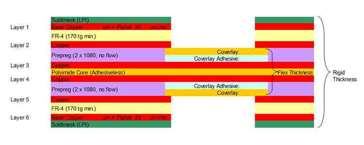
6 layer HDI flex PCB stackup example
Laser Drilling Microvias
Microvias in HDI flex are drilled with laser technology capable of vias down to 50 μm diameter or less. CO2 or UV lasers provide the fine accuracy needed.
Thin Film Metallization
Sputtered thin film metals create the traces and microvia barrels. Common finishes are electrodeposited copper and various organic surface finishes. These provide fine 15/15 μm traces and spaces.
High-Density Interconnects
HDI flex allows mounting of high-density components like fine pitch BGAs, CSPs, and flip chips. Common pad pitches reach down to 0.3 mm. Interconnects use microvias and thin traces.
Fine Line Patterning
Lithographic patterning transfers the circuit design onto the thin film layers. Stepper aligners provide accuracy down to 2 μm for tight line geometries.
Advanced QA
HDI flex fabrication requires advanced QA using 5D automated optical inspection (AOI) and other metrology tools. This ensures quality production of the fine features.
HDI Flex PCB Design Rules
To successfully implement HDI flex PCBs, engineers must design to the capabilities and limitations of HDI processes. Key design rules include:
Trace/Space
- Minimum trace width: 15 μm
- Minimum space: 15 μm
Microvias
- Finished diameter range: 50 – 100 μm
- Minimum annular ring: 25 μm
- Maximum aspect ratio: 1:1
Routing Layers
- 4-8 layers typical
- Minimum dielectric thickness: 25 μm
- Blind/buried vias used when possible
Component Land Patterns
- BGA pitch down to 0.3 mm
- Fine pitch perimeter and staggered array routing
Following HDI design rules ensures your board can be fabricated without defects. Work closely with your PCB manufacturer early in design to verify your layout adheres to their capabilities.
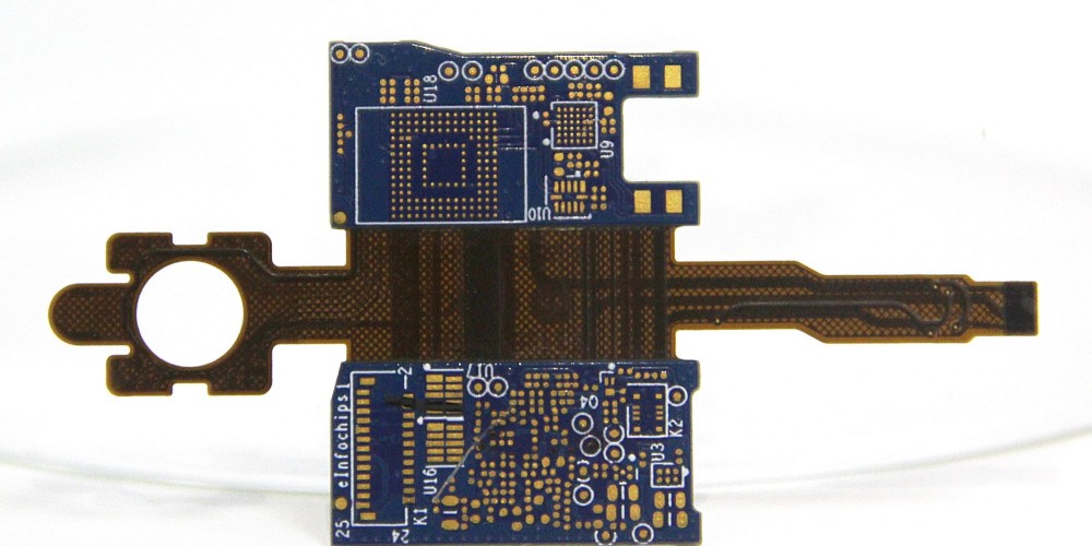
HDI Flex Applications
HDI flex PCBs enable solutions not possible with standard flex or rigid boards. Here are some common application areas:
Wearables
HDI flex is ideal for smartwatches, fitness trackers, VR/AR headsets, and other compact wearable devices. HDI provides the interconnect density for feature-packed designs.

HDI flex in a smartwatch application
Medical Electronics
Implantable and wearable medical devices use HDI flex for tight, multi-layer routing of sensors, power, and high-speed digital signals. The thin, flexible form factor conforms to the body.
Automotive Electronics
Automotive camera modules, car displays, sensor assemblies, and in-vehicle networking all utilize HDI flex PCBs. Rugged flexible circuits withstand vibration while fitting into tight spaces.
Consumer Electronics
Mobile phones, laptops, tablets, and other consumer electronics integrate HDI flex to interconnect advanced logic, memory, wireless, cameras, and displays. Enables more features in thinner devices.
Aerospace/Defense
Rugged flex-rigid assemblies with high density interconnects meet the demands of aerospace and defense electronics, while saving weight and space.
Benefits of Using HDI Flex PCBs
Here are some of the top advantages HDI flex PCB technology provides:
Size Reduction
HDI flex minimizes product size. More functionality fits into a smaller footprint. Thin, flexible circuits fold into tight spaces.
Increased Reliability
The flexible material withstands vibration, thermal cycling, and flexing stresses better than rigid boards. HDI design spreads traces across layers, improving redundancy.
Higher Speeds
Tighter trace geometries, thinner dielectrics, and laser microvias enable higher speed signals, above 10 Gbps. Signal integrity is enhanced.
Lighter Weight
Thin flexible circuits with microvias reduce weight versus rigid PCBs. Important for wearables, aerospace systems and portable electronics.
Design Freedom
Flexible circuits provide complete 3D design freedom. Dynamic flexing, folding, wrapping, and integrated assembly into packages is possible.
Lower Costs
HDI flex allows complexity consolidation, replacing connectors and simplifying assembly. Tighter integration lowers overall system cost.
Challenges of HDI Flex PCBs
While delivering major benefits, HDI flex also comes with some design and manufacturing challenges:
Increased Costs
The specialized processes required for laser drilling, thin films, and high-density patterning are more expensive compared to standard flex PCB fabrication.
Tighter Tolerances
HDI features down to 15 μm lines and spaces have much tighter tolerances than typical PCBs. This demands advanced QA processes.
Via Reliability
The miniscule microvias used in HDI flex are more prone to reliability issues like cracking under dynamic flexing. Careful design mitigation is required.
Limited Suppliers
Only advanced PCB fabricators can reliably produce HDI flex boards. Supply chain options are more limited compared to standard flex PCBs.
Complex Design
HDI flex requires following tight design rules and using advanced modeling and analysis tools. More upfront engineering work is needed.
HDI Flex Design Tips
Here are some best practices to follow when designing your HDI flex PCB:
- Work closely with your PCB manufacturer early in the design process. Have them review your preliminary layouts and stackup.
- Use their capabilities document for latest design rules, tolerances, and guidelines. Don’t assume standard rules apply.
- Model your high-speed signals. Use simulations and constraints to achieve signal integrity. Account for losses in thin dielectrics.
- Minimize dynamic rigid-flex transitions. Use wide radius curves and reinforcing layers at bends.
- Eliminate high aspect ratio filled microvias where possible. They can crack under flexing or drilling.
- Build in redundancy with parallel routes. This reduces risk of open circuits.
- Incorporate strain relief features into the flex portion. Use stabilizer layers or advanced techniques like tenting or slotting.
Conclusion
HDI flex PCBs provide interconnect solutions not achievable with standard flex or rigid technologies alone. By combining high density traces, microvias, and thin dielectrics on flexible circuit boards, HDI flex enables advanced functionality in compact, lightweight, and highly reliable designs.
Consumer demand for wearables, compact mobile devices, rugged electronics and other space-constrained applications will drive increasing adoption of HDI flex PCBs and Substrate-like PCBs (SLPs). Engineers should gain familiarity with the manufacturing processes, design guidelines, analysis techniques, and benefits of implementing HDI flex. Used appropriately, this disruptive technology can help enable the next generation of thin, fast, feature-packed electronic devices.
FAQ
What is the key difference between HDI flex and standard flex PCBs?
The main difference is HDI flex utilizes finer features like traces down to 15 μm widths, laser microvias below 50 μm diameter, and thinner dielectrics. This allows integration of more signals and components in a given area.
How many routing layers are typical for HDI flex PCBs?
Most HDI flex designs utilize 6-8 metal routing layers. Some may use up to 10 or more layers for advanced designs. This allows dense vertical interconnections.
Can components be mounted directly to HDI flex PCBs?
Yes, HDI flex is designed for direct surface mount attachment of components. Typical component pitches range down to 0.3 mm. Embedded die or chip-on-flex mounting can also be used.
Does HDI flex allow bends and dynamic flexing?
Properly designed HDI flex PCBs can bend and flex dynamically. Typical minimum bend radii range from 2-5 mm. Careful structural design is needed for reliability.
What are some key benefits of HDI flex PCB technology?
Main benefits include increased interconnect density, smaller and lighter circuits, enhanced reliability, higher speeds, design freedom, and cost savings through integration and miniaturization.