


Introduction
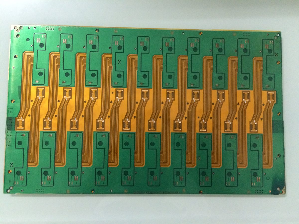
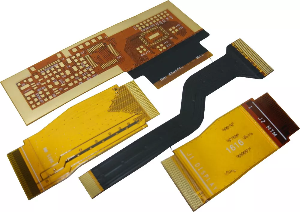
Rigid-flex PCBs integrate rigid PCB substrates with flexible circuit connections on the same board. This enables compact 3D form factors, allowing the rigid parts to host components while the flex sections provide interconnections between PCB sections. Rigid-flex boards open up new possibilities in product design and miniaturization for wearable devices, medical devices, industrial equipment, and consumer electronics.
However, working with rigid-flex PCBs also introduces additional complexity in the design and manufacturing process. Prototyping with rigid-flex requires special considerations in the mechanical and electrical design, material selection, layout, and assembly process. Errors can be costly if issues are only discovered after volume production begins.
This guide aims to provide a comprehensive overview of best practices, challenges, and solutions when prototyping with rigid-flex PCBs. We’ll cover key factors in the design phase, material selection, manufacturing preparations, assembly considerations, and testing. With the right knowledge and preparation, you can effectively prototype rigid-flex PCBs and avoid costly mistakes down the road.
Rigid-Flex Design Factors
Designing a rigid-flex PCB requires balancing electrical performance needs with the mechanical requirements for flexing, bending, and structural stability. Here are some key considerations:
Layer Stack Planning
- Determine the number of conductive layers needed, including the copper weight/thickness (common options are 1/1 oz, 1/2 oz, 2 oz)
- Select dielectric materials for the rigid and flex sections
- Ensure adequate thickness is planned for rigidity in rigid sections
- Minimize layers in flex areas to improve bendability
Circuit Layout
- Optimize component placement to minimize trace length
- Place fine-pitch components in rigid sections only
- Avoid traces in flexing regions whenever possible
- Allow adequate flex bend radius for traces crossing rigid-flex interfaces
- Use teardrop pads for traces connecting rigid to flex sections
Mechanical Factors
- Determine required bend radius for flex areas based on dielectric material
- Ensure rigid sections are adequately large for component mounting
- Use stiffeners/supports under components or high stress areas
- Manage thermal expansion differences between rigid and flex sections
Testability
- Include fiducials and testpoints to support prototyping and testing
- Plan for access to interfaces needed for programming and debugging
- Consider using interposers or test sockets to allow access to small components
Material Selection
Choosing the right materials is crucial when designing a rigid-flex PCB. Key factors to consider:
Dielectric Flex Materials
Popular options:
- Polyimide (Kapton) – Low cost, good flex life and chemical resistance
- PTFE (Teflon) – Excellent chemical resistance, higher frequency support
- Polyester (PET) – Low moisture absorption
- LCP (liquid crystal polymer) – Stable electrical performance in high frequency circuits
Considerations: Flexibility, bend radius, chemical resistance needed, moisture absorption, frequency support, cost
Rigid Substrate Materials
Common alternatives:
- FR-4 – Affordable, suitable for many consumer electronics
- High-Tg FR-4 – Improved thermal and mechanical performance
- Halogen-free/green materials – Environmentally friendly
- CEM-1, FR-5, G-10, polyimide – For more demanding applications
Considerations: Dielectric constant, loss tangent, Tg, thermal conductivity, CTE, cost
Copper Foil
- 1/1 oz and 1/2 oz most common weights for flex and outer layers
- 2 oz foils often used for inner layers on rigid sections
- Rolled copper foil preferred for flex vs. electrodeposited
- Special foils like ITF (Inversely Truncated Fine) improve flex cracking resistance
Coverlay/Coverfilm
- Polyimide commonly used for fabricating the coverlay (protective coating over conductors)
- Adhesive selection impacts properties like flex life, chemical resistance, strength
Mechanical Design Guidelines
Optimizing the physical layout and managing mechanical stress is key to ensuring the reliability of rigid-flex prototypes. Here are some guidelines:
Layer Transitions
- Taper layer transitions between rigid and flex sections for reliability
- Allow sufficient clearance around edges of rigid sections attaching to flex
Bend Radii
- Follow minimum bend radius guidelines from material suppliers
- Typical minimum inside bend radius is 3-10X dielectric thickness
- Tight folds under 1X thickness can crack flex layers
Flex Stiffeners
- Stiffeners made of coverlay or adhesive can help manage flex stress
- Place stiffeners around holes or high stress areas
- Stiffeners improve tear resistance during repeated flexing
Corner Design
- Use rounded corners instead of 90 degree angles on rigid sections attaching to flex
- Dogbone cutouts can also relieve stress at corners
Component Placement
- Avoid placing heavy, large or high-profile components in flexing sections
- Balance weight distribution to avoid excessive torsional stress
Teardrop Pads
- Use teardrop shaped pads for traces connecting rigid to flex areas
- Improves reliability of traces crossing material transitions
Following these guidelines will help create mechanically robust rigid-flex prototypes and avoid issues like cracks, separation between layers, component detachment, and PCB flex damage.
Layout and Stackup Design
Rigid-flex stackup design follows the same principles as multilayer PCB stackups, with considerations for:
- Signal routing layers placement
- Reference planes for controlled impedance
- Power distribution layers
- Balanced symmetrical stackups to avoid warpage
Some additional factors for rigid-flex:
- Add additional dielectric layers in rigid sections vs. flex regions
- Assign layers dedicated for shielding flex regions. Flex sections are prone to EMI.
- Use thicker 2 oz copper for power distribution layers in rigid sections
- Keep high speed routing layers closer to surface on outer layers of flex regions
- Assign ground layers next to shielded flex sections
Here is an example 6-layer rigid-flex stackup:
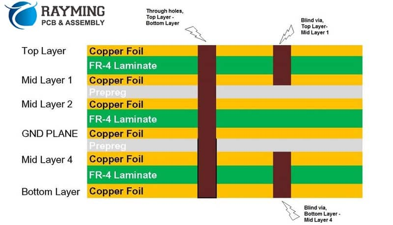
This provides controlled impedance routing layers, robust power distribution, and shielded flex sections.
For the layout:
- Use wider trace widths and spacing in flex sections
- Avoid traces perpendicular to bend axis
- Place components on one side of flex sections whenever possible
- Route critical signals on outer layers of rigid sections
Manufacturing and Assembly
Preparing for manufacturing rigid-flex prototypes requires attention beyond typical PCB fabrication to ensure success:
Panel Design
- Utilize panel sizes supported by manufacturer equipment
- Efficiently arrange boards to maximize panel utilization
- Include fiducials, test points, and breakaway tabs
Layer Registration
- Tight registration tolerances are needed, around 0.075mm
- Should be confirmed by fabricator based on their process capabilities
Via Protection
- Protective tenting should be used for any vias in flexing areas
- Prevents stress concentration on via barrels
Copper Balancing
- Aim for equal copper thickness on top and bottom of flex layers
- Helps avoid curling from uneven thermal expansion and contraction
Testability
- Include testpoints for access during assembly and debug
- Breakaway sections can allow connecting probes
Tooling and Fixtures
- Programming-enabled test fixtures are recommended for assembly
- Guide plates or frames help support flex sections
Assembly Process
- Soldering should be done in static, not dynamic flex state
- Adhesives improve component support in flex sections
- Spot apply adhesive at component edges for shear strength
- Light score lines guide and limit flexing to intended hinge points
With attention to these areas, PCB assemblers can avoid issues like cracking, warpage, layer misalignment, and damage to components or flex interconnects.
Functional Testing
Verifying the design early helps catch issues while changes are still inexpensive during prototyping.
Key tests to conduct:
- Automated optical inspection of solder joints
- X-ray inspection to check inner lamination alignment
- ICT testing for shorts, opens, and proper connections
- Continuity tests of flex interconnects during dynamic flexing
- HASS testing of bend cycles and mechanical durability
- Visual inspection of rigid-flex junctions
- Impedance testing of high speed traces
- Functionality testing in final enclosure and form-factor
FQA
How many bend cycles can a typical rigid flex board support?
The bend cycle lifetime depends on several factors like the flex material, stiffness, bend radius, and environment. With optimal design, many rigid-flex boards can reliably withstand 500 – 5000+ dynamic bend cycles before failure. Critical applications will subject prototypes to bend testing under accelerated life test conditions to validate cycles exceed product requirements.
What clearance should be allowed around rigid sections attached to flex?
A minimum clearance of at least 0.4mm around rigid sections adjoining flex areas is recommended. This helps avoid stress concentrations that can delaminate layers.
Are via-in-pad designs acceptable on rigid-flex boards?
Via-in-pad can improve routing density but is not recommended for rigid-flex because it can concentrate flexing stress at the vias leading to cracking. The recommended approach is to place any vias near pads instead of in pads.
How are components attached to flexing sections?
Soldering is not reliable long-term in dynamic flex zones. Adhesives like epoxies or acrylics should be used to attach components to flexing regions. This provides shear strength to prevent components detaching.
What are recommended soldering methods for rigid-flex boards?
Reflow soldering is preferred over wave soldering for rigid-flex assemblies. The board should be soldered in a static, not flexed state, and adhesive used to augment soldered components in flex zones. Dual-stage reflow profiles ensure compatibility with flex dielectric materials.
In summary, rigid-flex PCB prototyping requires upfront planning, specialized materials and processes, and careful validation testing to ensure reliable performance. Following the guidelines in this article will help you successfully prototype your rigid-flex product designs. Let me know if you have any other questions!