

Manufacturing
Introduction
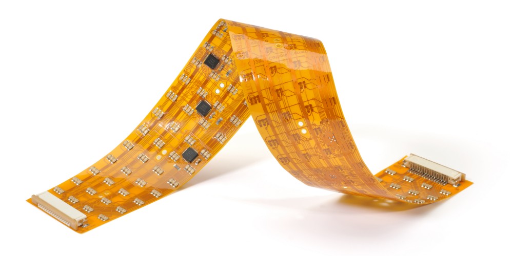
Polyimide flex PCBs, also known as flex circuits or flexible printed circuits (FPCs), are a type of printed circuit board made with a polyimide base material that provides flexibility. Polyimide has high heat and chemical resistance and is well-suited for flex PCB applications that require repeated bending cycles. Compared to rigid PCBs, polyimide flex PCBs can fit into tight spaces, allow for complex 3D form factors, and improve reliability in dynamic flexing environments. This article provides an overview of polyimide flex PCB technology, design considerations, manufacturing processes, and applications.
What is Polyimide?
Polyimide is a polymer material with high thermal stability. The stable aromatic structure of the polyimide molecular chains gives the material its distinctive thermal and chemical resistance properties. Polyimide film can withstand temperatures up to 300°C with minimal property degradation.
The two most common types of polyimide used for flex PCBs are:
- Kapton: Developed by DuPont, Kapton polyimide film offers a balance of electrical, mechanical, chemical, and high temperature properties. It has excellent dimensional stability during flexing.
- UPILEX: A polyimide film from Ube Industries noted for its very low thermal expansion coefficient, a property important for precision flex circuit layouts.
Compared to other common flex circuit substrates like PET and PEN, polyimide has much higher working temperatures with lower thermal expansion, better chemical resistance, and stronger dielectric properties.
Benefits of Polyimide Flex PCBs
There are several advantages to using a polyimide-based flex PCB over a rigid printed circuit board:
- Flexibility: Polyimide flex circuits can bend repeatedly to fit and dynamically flex in space-constrained applications. The flex life relates to the circuit’s bend radius vs thickness.
- Lightweight: Polyimide flex PCBs are thinner and lighter than rigid PCBs. This helps reduce assembly weight.
- 3D assembly: Flex circuits can be folded, wrapped, rolled, and formed into complex 3D shapes for compact, efficient electronic packaging.
- High frequency: Polyimide has low signal loss at high frequencies compared to other polymer substrates, a benefit for high-speed applications.
- Reliability: Dynamic flexing reduces mechanical stress and failures associated with vibration, shock, and temperature fluctuations.
- Miniaturization: Fine line traces allow high component densities and miniaturization of flex circuit assemblies.
In short, polyimide flex PCB technology enables smaller, lighter, and more reliable electronics and interconnects. The design freedom facilitates denser, more compact products and assemblies.
Design Considerations
Designing a polyimide flex PCB requires special considerations for the flexible substrate. Here are some of the most important flex PCB design guidelines:
- Bend radius: Avoid tight folds and aim for bend radii at least 10x the circuit thickness for longer flex life. Consider dynamic folding requirements.
- Layer stackup: Stiffer layers or adhesives can be added to create more robust flex-rigid combinations. Manage total thickness.
- Circuits layouts: Follow trace width/space rules for controlled impedance. Annular ring requirements differ. Plan for flex-to-rigid transitions.
- Component mounting: Use specifically designed flex component packages. Allow clearance for dynamic flexing range of motion.
- Conductive layers: 1-2oz electrodeposited copper with nickel/gold plating for corrosion resistance and reliability. Strain-relief patterns can help.
- Board stiffening: Strategically place board stiffeners, shields, or metal backing to enable robust handling. Manage board stiffness vs flexibility.
- ESD/EMR: Plan for electromagnetic shielding, isolation, and protective coatings as needed. Ground planes help shield signals.
With careful planning and rules compliance, polyimide flex PCBs can be designed to balance optimal electrical performance, reliability, and flexibility.
Manufacturing Process
Polyimide flex PCBs use a sophisticated fabrication process with many specialized process steps to create a robust flex circuit assembly. Here is a general overview of the flex PCB manufacturing process:
- Substrate preparation – Ultrathin polyimide film is cut to size and cleaned. Adhesive coating or stiffeners layers can be added.
- Photolithography – Photoresist is coated on the polyimide surface and imaged to define the circuit pattern.
- Etching – Exposed copper is etched away, leaving only the desired conductor traces/pads.
- Resist stripping – The remaining photoresist is removed from the base polyimide film.
- Dielectric coating – Polyimide coatings are layered between circuits for electrical isolation.
- Via formation – Holes are etched or laser-drilled in the dielectric layers to form interlayer connections.
- Plugging/metallization – Vias are plated with conductive material for vertical interconnections between layers.
- Circuit patterning – Additional circuit layers are processed using the photolithography steps above. Multilayer circuits are built up sequentially.
- Component assembly – Bare die/components are assembled onto the flex PCB using soldering, conductive epoxy, ultrasonic welding etc.
- Testing – Continuity, open/short circuits, and functional tests ensure quality prior to shipment.
Flex PCB production requires specialized equipment, chemical formulations, and process controls to handle the thin, flexible polyimide substrates.
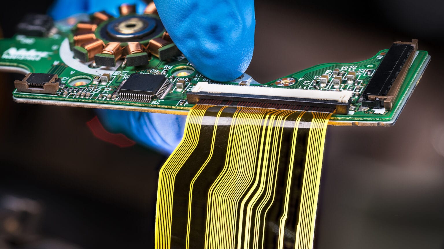
Flex-to-Rigid PCB Combinations
For many applications, flex PCBs attach to standard rigid PCBs. The combination allows for a rigid PCB to connect to a dynamic flexing interconnect.
There are several flex-to-rigid PCB attachment techniques:
- Soldered connections – Flex circuits terminals are soldered to pads on rigid PCBs. Careful strain relief design is needed.
- Mechanical clamps – Screws, rivets or clamps provide removable flex PCB connections to rigid boards.
- Adhesive bonding – Acrylic or epoxy adhesives permanently bond flex to rigid PCBs. Ease of repair is limited.
- ZIF/LIF connectors – Zero insertion or low insertion force connectors allow detachable flex connections without soldering.
- Anisotropic conducting films – ACF bonds flex circuits and only conducts through vertical pressure connections. Re-workable.
The joints between rigid and flexing PCB regions often see the most stresses. Flex-to-rigid connectors must manage these interfaces for long life operation.
Applications of Polyimide Flex Circuits
Polyimide flex PCBs are used across many industries from consumer electronics to aerospace systems. Some common applications include:
- Wearable devices – watches, fitness trackers, health monitoring devices
- Mobile phones – chip-on-flex packaging, hinge or slide interconnects
- Automotive – camera/sensor flex cabling, seat heaters, door wiring
- Medical – hearing aids, patient monitors, surgical equipment
- Defense – avionics, missiles, soldier systems, UAVs
- Space systems – satellite components, solar arrays, antennae
- Computing – foldable/rollable displays, disk drive flex interconnects
- Robotics – moving joints, head/arm/gripper wiring
Polyimide flex circuits can dynamically interconnect electronic assemblies where movement, space constraints, or reliability are important requirements. Continued improvements in polyimide materials and flex PCB fabrication promise to open additional application spaces.
Frequently Asked Questions
What are some key differences between rigid PCBs vs polyimide flex PCBs?
Rigid PCBs use thicker, FR4 glass epoxy substrates for structural support, while flex PCBs use thin polyimide films down to 12 microns for flexibility. Flex circuits can dynamically bend, while rigid PCBs are static. The fabrication process also differs with specialized steps to handle polyimide. The circuit design rules vary to accommodate dynamic flexing.
How flexible can polyimide flex circuits be?
Polyimide flex PCBs can be bent to radii down to 3-5x the total thickness. Typical flex life expectancies are 10,000-100,000+ cycles depending on thickness and bend radius. Dynamic folding applications require expert design to avoid fatigue or cracks.
How many layers can polyimide flex PCBs support?
While rigid boards may have 20+ layers, present flex PCB technology typically supports 4-6 conductive layers, including outer copper layers. Improved laser drilling and metallization techniques continue to increase the achievable number of flex circuit layers.
Can components be mounted directly on polyimide flex PCBs?
Yes, but component packaging must be designed for flex PCB assembly. Standard leaded or SMT component packages can fracture under bending stresses. Special package styles like bare die/flip chip or land grid array are often used. Clearance is designed for dynamic component motion.
How are polyimide flex PCBs tested?
Flex circuits undergo electrical testing like opens/shorts checks, netlist verification, and functional validation on specialized fixtures allowing for dynamic bending during test. Automated optical inspection and x-ray imaging are used for quality control. Careful handling procedures are required.
Conclusion
Polyimide flex PCBs enable tight, lightweight, and reliable electronics interconnects thanks to the robust thermal and chemical properties of the polyimide film substrate. When designed with proper bend radius, layer stackup, and layout rules, polyimide flex circuits can achieve millions of flex life cycles for dynamic applications. Continued improvements in flex PCB technology and fabrication will further the capabilities and market reach.