


ntroduction
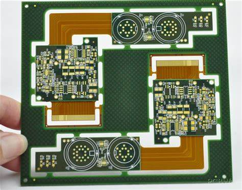
Rigid-flex PCBs integrate rigid and flexible materials into a single circuit board assembly. They allow the rigid sections to provide mechanical support while the flexible sections enable dynamic flexing and bending. Rigid-flex PCBs are ideal for applications where size, weight, and reliability are critical such as aerospace, automotive, medical, consumer electronics and more.
Altium Designer provides a complete set of tools to design rigid-flex PCBs. This guidebook covers the key features and workflows in Altium to successfully design a rigid-flex board.
Rigid-Flex Design Features
Layer Stack Manager
The Layer Stack Manager is used to define the layer structure. It allows you to specify rigid and flex layer sections.
- Rigid layers are assigned to a Region Layer Span.
- Flex layers span across regions.
- Mechanical layers like cover layers can also be defined.
- Different layer stacks can be used in different board regions.
Defining Regions
The Regions define the rigid and flex areas of the PCB.
- Set the region layer to the mechanical layer span defined earlier.
- Specify the region type – Rigid or Flex.
- Define region shapes and dimensions.
Component Placement
- Components are restricted to rigid regions for support.
- Use region commands to check/filter components placement.
- Inter-region gaps provide flex clearance. Adjust to control bend radius.
Routing
- Follow existing PCB routing features.
- Control bend radii in flex areas.
- Manage different width requirements in rigid vs. flex areas.
3D Modeling
- Model rigid sections as simple extruded cutouts.
- Model flex sections using complex 3D shapes to represent live flexing.
- Verify clearances.
Rigid-Flex Design Checklist
Follow this checklist for a successful rigid-flex design:
Project Setup
- Choose flex board technology.
- Include flexible substrate layer(s).
- Define discrete layer stacks for rigid and flex regions.
Board Outline
- Draw overall board profile.
- Define mechanical layers for coverlay.
Regions
- Add regions for rigid and flex sections.
- Assign region layer and type.
Placement
- Place components only in rigid regions.
- Mind gaps between regions.
Routing
- Enable teardrop pads and beveled traces.
- Control trace width changes between rigid and flex.
- Set appropriate bend radii where traces cross into flex regions.
3D Model
- Model rigid sections with simple extruded cutouts.
- Use complex shapes to model live flexing in the flex regions.
Example Rigid-Flex Design
Here is an example rigid-flex design with details on the key steps:
Layer Stackup
- Layer stack has discrete sections for the 2 rigid and 1 flex region.
- Flex layers span across regions.
- Cover layers defined as mechanical layers.
Regions Defined
- Board divided into Rigid1, Flex, and Rigid2 regions.
- Region layer is the cover layer.
Component Placement
- Components placed only in rigid sections.
- Gap kept between rigid regions for flex bend area.
Routing
- Traces routed normally in rigid sections.
- Bend radius controlled where traces enter flex region.
- Trace widths adjusted to match rigid/flex requirements.
3D Model
- Rigid sections modeled as simple extruded cutouts.
- Complex curvature added to model flexing in the flex region.
This example illustrates the key concepts and workflow to design a rigid-flex PCB in Altium Designer. The layered approach with well-defined regions enables a smooth and accurate implementation.
Frequently Asked Questions
What are the typical applications for rigid-flex PCBs?
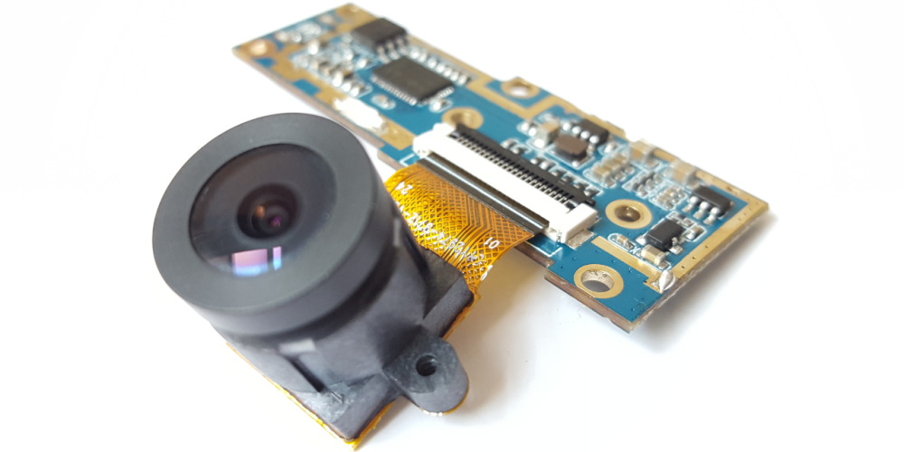
Rigid-flex PCBs are well-suited for applications where flexibility is required like wearables, medical devices, consumer electronics, aerospace systems, automotive cameras, etc. The rigid sections provide mechanical support while the flex areas enable contour matching and dynamic flexing.
What are the main benefits of a rigid-flex design?
Key benefits are reduction in weight, size, and layers compared to discrete rigid and flex boards. They also improve reliability by minimizing interconnections. The ability to embed components gives higher density. Lower cost compared to complex flex assemblies.
What are the minimum bend radius and trace width rules?
Minimum bend radius is usually set at 3-10 times the total board thickness depending on the substrate. Trace widths in flexible sections are normally higher (~0.2 mm) compared to rigid sections due to dynamic flexing.
How is impedance controlled in the flex sections?
Maintain at least 2-3 unbroken ground planes below flex sections. Use thicker dielectric material if lower impedance is needed. Planes provide capacitance for impedance control.
How to transition components between rigid and flex sections?
Use tented or beveled vias at rigid-flex intersections. Flat vias can crack under dynamic flexing. Special pad shapes that facilitate flexing should be used.
Conclusion
Rigid-flex PCBs provide great benefits for designs requiring flexibility and reliability. Altium Designer offers advanced tools to model and integrate rigid and flex sections in one PCB assembly. With careful planning and execution, rigid-flex technology can help produce lightweight and robust electronic devices.