

What is PCB Design?
PCB design is the process of creating printed circuit boards (PCBs) that electrically connect and mechanically support electronic components using conductive pathways, tracks, or signal traces etched from copper sheets laminated onto a non-conductive substrate. PCB design involves the creation of schematic diagrams, component placement, trace routing, and generation of manufacturing files.
The PCB design process typically includes the following steps:
- Schematic capture
- Component placement
- Trace routing
- Design rule checking (DRC)
- Generating manufacturing files
Schematic Capture
Schematic capture is the first step in PCB design. It involves creating a schematic diagram that represents the electrical connections between components. The schematic diagram is a graphical representation of the circuit and includes symbols for each component and lines representing the connections between them.
Component Placement
After creating the schematic, the next step is to place the components on the PCB layout. This involves arranging the components in a way that minimizes the size of the board while ensuring that the components are easily accessible for soldering and testing.
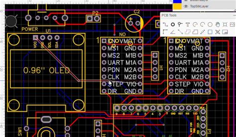
Trace Routing
Once the components are placed, the next step is to route the traces that connect them. Traces are the conductive pathways that carry electrical signals between components. The goal of trace routing is to create the shortest possible paths between components while avoiding interference and ensuring that the traces are wide enough to carry the required current.
Design Rule Checking (DRC)
After the traces are routed, the next step is to perform a design rule check (DRC). The DRC checks the PCB layout against a set of predefined rules to ensure that it meets the manufacturing requirements. These rules include minimum trace widths, minimum clearances between traces, and minimum hole sizes.
Generating Manufacturing Files
The final step in PCB design is to generate the manufacturing files. These files include the Gerber files, which are used to create the photomasks for the PCB manufacturing process, and the drill files, which specify the locations and sizes of the holes to be drilled in the board.
PCB Design Considerations
When designing a PCB, there are several important considerations to keep in mind. These include:
Signal Integrity
Signal integrity refers to the quality of the electrical signals transmitted through the PCB. To ensure good signal integrity, it is important to minimize crosstalk, reflections, and other sources of noise. This can be achieved through proper trace routing, impedance matching, and the use of ground planes.
EMI/EMC
Electromagnetic interference (EMI) and electromagnetic compatibility (EMC) are important considerations in PCB design. EMI refers to the unwanted electrical noise generated by the circuit, while EMC refers to the ability of the circuit to operate correctly in the presence of external electromagnetic fields. To minimize EMI and ensure EMC, it is important to use proper shielding, filtering, and grounding techniques.
Thermal Management
Thermal management is another important consideration in PCB design. Electronic components generate heat during operation, and if this heat is not properly dissipated, it can lead to component failure and reduced reliability. To ensure proper thermal management, it is important to use adequate copper pours, thermal vias, and heatsinks where necessary.
Manufacturing Constraints
Finally, it is important to consider the manufacturing constraints when designing a PCB. These constraints include the minimum trace widths, minimum clearances, and minimum hole sizes that can be achieved with the available manufacturing processes. It is important to design the PCB with these constraints in mind to ensure that it can be manufactured reliably and cost-effectively.

PCB Design Software
There are many software tools available for PCB design, ranging from simple schematic capture tools to complex multi-layer PCB design suites. Some of the most popular PCB design software tools include:
| Software | Description |
|---|---|
| Altium Designer | A comprehensive PCB design suite with advanced features for high-speed design and simulation. |
| KiCad | A free and Open-source PCB design suite with schematic capture, PCB layout, and 3D viewing capabilities. |
| Eagle | A popular PCB design tool with a large component library and support for automated routing. |
| OrCAD | A powerful PCB design suite with advanced simulation and analysis capabilities. |
| DesignSpark PCB | A free PCB design tool with a simple user interface and built-in component libraries. |
When choosing a PCB design software tool, it is important to consider factors such as ease of use, feature set, cost, and compatibility with your existing design workflow.

PCB Manufacturing
Once the PCB design is complete, the next step is to manufacture the board. PCB manufacturing involves several steps, including:
- PCB fabrication
- PCB Assembly
- Testing and inspection
PCB Fabrication
PCB fabrication is the process of creating the bare PCB from the design files. This typically involves the following steps:
- Creating the photomasks from the Gerber files
- Coating the copper-clad laminate with a photoresist
- Exposing the photoresist to UV light through the photomasks
- Developing the photoresist to remove the unexposed areas
- Etching away the exposed copper to create the traces
- Drilling the holes specified in the drill files
- Applying a solder mask and silkscreen to the board
PCB Assembly
After the bare PCB is fabricated, the next step is to assemble the components onto the board. This typically involves the following steps:
- Applying solder paste to the pads on the PCB
- Placing the components onto the pads
- Reflowing the solder paste to create a mechanical and electrical connection between the components and the PCB
- Cleaning the board to remove any flux residue
Testing and Inspection
After the PCB is assembled, it is important to test and inspect the board to ensure that it functions correctly. This typically involves the following steps:
- Visual inspection to check for any obvious defects or damage
- Electrical testing to verify that the board functions as intended
- Functional testing to ensure that the board meets the required specifications
- Environmental testing to ensure that the board can withstand the expected operating conditions

PCB Design Services
For companies that do not have the expertise or resources to design PCBs in-house, there are many PCB design services available. These services typically offer a range of options, from simple schematic capture and PCB layout to full turnkey design and manufacturing.
When choosing a PCB design service, it is important to consider factors such as:
- Experience and expertise in your specific industry or application
- Quality of the design process and resulting PCBs
- Turnaround time and cost
- Communication and customer support
Some popular PCB design services include:
| Service | Description |
|---|---|
| Sierra Circuits | A full-service PCB design and manufacturing company with expertise in high-speed, RF, and flexible circuits. |
| Royal Circuits | A PCB design and manufacturing service with a focus on quick-turn prototyping and low-volume production. |
| Advanced Circuits | A leading PCB manufacturer with a free PCB design tool and a variety of manufacturing options. |
| PCBWay | A global PCB manufacturer with a range of PCB design and assembly services. |
| Sunstone Circuits | A PCB Prototyping and manufacturing service with a focus on high-quality, reliable PCBs. |
FAQ
What is the difference between a PCB and a printed wiring board (PWB)?
A PCB and a PWB are essentially the same thing. Both terms refer to a board that is used to mechanically support and electrically connect electronic components using conductive pathways, tracks, or signal traces. The term “PCB” is more commonly used in the industry today.
What are the different types of PCBs?
There are several types of PCBs, including:
- Single-sided PCBs: These have components and traces on only one side of the board.
- Double-sided PCBs: These have components and traces on both sides of the board, with through-hole connections between the sides.
- Multi-layer PCBs: These have multiple layers of traces and insulating material, allowing for more complex circuits and higher component density.
- Flexible PCBs: These are made from flexible materials and can be bent or folded to fit into tight spaces.
- Rigid-Flex PCBs: These are a combination of rigid and flexible PCBs, with rigid sections connected by flexible sections.
What is the typical turnaround time for PCB design and manufacturing?
The turnaround time for PCB design and manufacturing can vary depending on the complexity of the design, the manufacturing process used, and the workload of the design and manufacturing teams. For simple designs and quick-turn prototyping, the turnaround time can be as short as a few days. For more complex designs and higher volumes, the turnaround time can be several weeks or longer.
What are some common PCB design mistakes to avoid?
Some common PCB design mistakes to avoid include:
- Not considering the manufacturing constraints and capabilities of the PCB fabricator
- Not properly managing the power and ground planes, leading to noise and signal integrity issues
- Not adequately protecting the PCB from electromagnetic interference (EMI) and electrostatic discharge (ESD)
- Not properly documenting the design, making it difficult to troubleshoot and maintain the PCB
- Not testing the PCB thoroughly before production, leading to costly redesigns and delays
How much does PCB design and manufacturing cost?
The cost of PCB design and manufacturing can vary widely depending on factors such as the complexity of the design, the number of layers, the size of the board, the manufacturing process used, and the volume of boards produced. For simple designs and low volumes, the cost can be as low as a few dollars per board. For more complex designs and higher volumes, the cost can be several hundred or even thousands of dollars per board. It is important to work closely with your PCB design and manufacturing partners to understand the costs involved and to find ways to optimize the design and manufacturing process for your specific needs and budget.