

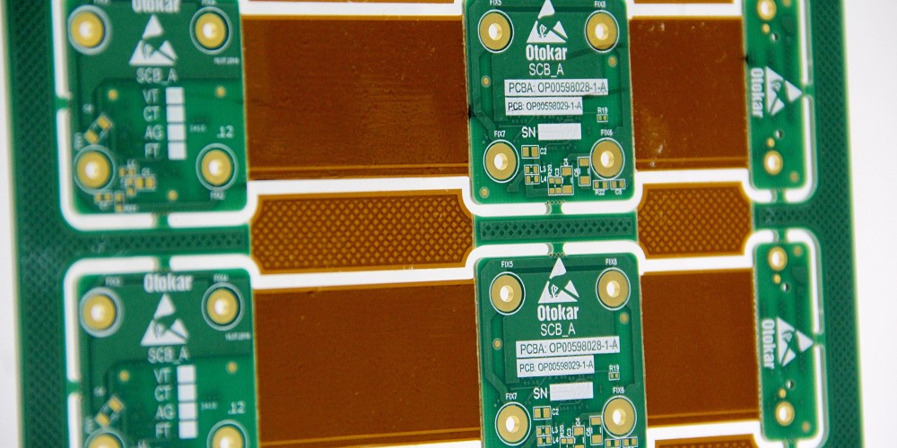
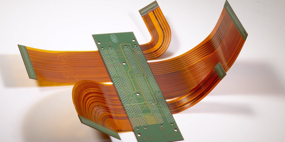
Overview of Rigid Flex PCBs
A rigid flex PCB is a printed circuit board that consists of both rigid and flexible substrates laminated together. The rigid sections provide mechanical support while the flexible sections allow dynamic flexing and bending. Rigid flex PCBs provide several advantages:
- Allows 3D configuration and dense interconnections
- Can fit into small and complex devices
- Accommodates motion or vibration
- Reduces system wiring and connectors
Rigid flex PCBs are widely used in aerospace, military, medical, consumer electronics and automotive applications. The most common flexible substrate materials are polyimide and PEEK. Popular rigid substrate materials include FR-4, CEM-1, polyimide and ceramic.
Rigid Flex PCB Design Considerations
Designing a rigid flex PCB in Altium requires special considerations:
Layer Stackup
The layer stackup defines the substrate materials, copper layers, and dielectric materials used to separate copper layers. Rigid layers often use FR-4 while flex layers use polyimide or PEEK. Adhesive layers bond the rigid and flex layers together.
Bend Radius
The minimum bend radius depends on the flex layer material. Polyimide typically allows a bend radius around 5x the flex layer thickness. Too tight of a bend radius can crack soldermask and copper traces.
Component Placement
Components should be placed primarily on rigid sections. Some passive components like resistors and capacitors can be placed on flex areas. Larger ICs should be placed on rigid areas or “islands”.
Routing
Traces should be routed along the rigid sections as much as possible. Use 45° angles instead of 90° bends when crossing from rigid to flex. Avoid traces perpendicular to the bend axis.
Vias
Minimize the number of vias in the bend areas. Use tear-drop shapes at the end of traces near vias. Fill thermal vias in rigid sections for heat dissipation.
Stiffeners
Add stiffeners made of rigid material to strengthen the flex area against bending stresses. Use teardrop shapes at the end of stiffeners to reduce stress points.
Soldermask
Define soldermask pullback from pads to prevent cracking. Soldermask should overlap any tear drops. Define soldermask openings in rigid areas for solderpaste and reflow.
Designing a Rigid Flex PCB in Altium
Here are the key steps to design a rigid flex PCB in Altium Designer:
1. Create Layer Stackup
Define the layer stackup through the Layer Stack Manager including rigid, flex, and adhesive layers along with dielectric materials. Set the bending stiffness for each layer.
2. Define Mechanical Layers
Add mechanical layers for the rigid/flex outline, board profile, 3D body, and assembly details.
3. Design Rigid and Flex Regions
Use Rigid-Flex design mode. Define the rigid and flex region outlines. Use middle-click to contour the rigid-flex boundary.
4. Place Components
Place components primarily on the rigid regions. Use attachment pads to secure large components crossing regions.
5. Route Traces
Route traces perpendicular to the bending axis when crossing between rigid and flex. Use tear drops at rigid/flex boundaries.
6. Define Cutouts
Use cutouts to create openings in rigid sections surrounded by flex layers. This helps reduce stresses.
7. Add Stiffeners
Add rectangular rigid stiffeners using the Stiffener tool. Use teardrops to reduce stress points.
8. Generate Design Output Files
Rigid-Flex mode creates outputs tailored for rigid flex manufacturing including documentation, fabrication, and assembly drawings.
Key Settings for Rigid Flex PCBs in Altium
Here are some of the important settings when designing rigid flex PCBs in Altium:
Layer Stack Manager: Define materials, layer types (rigid/flex), and dielectric specifications.
Bending Properties: Set the bending radius and stiffness for flex layers.
Mechanical Layers: Board Outline, 3D Body, Assembly Details etc.
Rigid-Flex Settings: Specify parameters like corner smoothing, teardrop size, scoring tolerance.
Plane Connect Style: Set connectivity rules between power planes crossing rigid/flex boundaries.
Component Placement: Use multi-board assembly components and room definitions.
Routing: Enable tear drop stubs, set track width design rules.
Design Rules: Define fiducials, annular rings, via styles, etc.
Manufacturing Outputs: Set file formats and options for documentation, fabrication, and assembly.
Properly configuring these settings ensures that the rigid flex design meets manufacturing and reliability requirements.
FAQ
What are some typical applications of rigid flex PCBs?
Rigid flex PCBs are commonly used in aerospace systems, portable electronics, optics assemblies, printer mechanisms, robotics actuators, and automotive cameras. The ability to embed flexible connections allows dense, motion-enabled electronics.
How many layers can rigid flex PCBs support?
Rigid flex PCBs can support over 20 layers with a mixture of rigid and flex layers. The rigid sections provide multilayer support while thin flex layers allow dynamic bending. High layer counts provide enhanced routing density.
What are some good flex layer materials?
Common flexible substrate materials include polyimide (PI), polyimide, PEEK, PET, and PEN. Polyimide is the most popular choice due to its electrical performance, thermal resistance, and flex durability.
What are some common problems with rigid flex PCBs?
Potential issues include cracked traces or soldermask, flex layer delamination, component detachment in flex areas, and broken plated through holes around bends. Careful design rules and testing helps avoid these failure modes.
How are components assembled onto rigid flex PCBs?
SMT components are assembled in the rigid PCB sections using standard SMT assembly processes. Through-hole components can be manually assembled in rigid regions. Glue or underfill is often used to strengthen connections of components bridging multiple PCB regions.
In summary, rigid flex PCB technology enables innovative 3D electronics design with the combination of rigid support and dynamic flex. Altium provides powerful tools to manage the complexity and outputs involved in rigid flex PCB design. By following best practice design guidelines, engineers can successfully develop rigid flex circuits for demanding applications.