

Introduction to Rigid Flexible PCBs
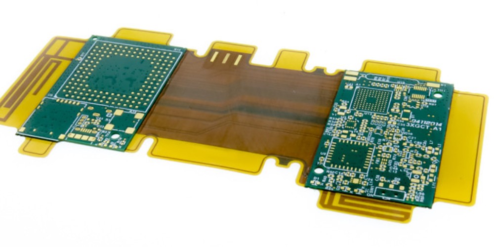
A rigid flexible printed circuit board (rigid flex PCB) combines rigid and flexible circuit boards into a single structure. As the name suggests, rigid flexible PCBs provide both rigidity and flexibility in the design. The rigid sections provide mechanical support while the flexible sections allow dynamic fit and 3-dimensional configuration.
Rigid flexible PCBs contain layers of flexible dielectric materials like polyimide along with layers of rigid fiberglass reinforced epoxy laminate materials. Conductive tracks are etched on the layers to create electrical connections. Vias and plated through holes provide conductivity between the layers.
Key Benefits of Rigid Flex PCBs
- Space saving design – By folding and bending, rigid flex PCBs fit into tight spaces
- Improved reliability – Eliminates interconnections between separate rigid and flex PCBs
- Reduced system assembly cost – Fewer components to assemble
- Enhanced flexibility – Dynamic movement and adjustments possible
- Light weight – Thin polyimide flexible layers reduce weight
Rigid flex PCBs are ideal for applications like cameras, computer displays, hard disk drives, robots, medical devices, aerospace electronics, etc. The combo design is especially useful when the electrical components and connectors are mounted on a rigid surface and interconnections are made via flexible printed circuits.
Rigid Flex PCB Construction
The construction of a rigid flex PCB involves laminating flexible copper clad dielectric films like polyimide with rigid prepreg or cores like FR-4. This creates a multilayer structure with both rigid and flexible layers bonded together.
Here are the common construction elements used in rigid flex PCBs:
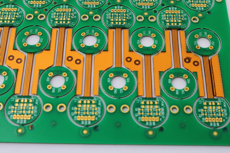
Flex Layers
The flex layers provide flexibility and are made up of a flexible polyimide base dielectric film clad with copper on one or both sides. Typical thickness of the polyimide film is between 25-100μm. Common flex layer stacks are:
- Single Sided Flex – Flexible layer, adhesive, copper on one side
- Double Sided Flex – Flexible layer, copper, adhesive, copper
Rigid Layers
The rigid parts of the PCB provide mechanical support and stability. Rigid layers are typically made of glass reinforced epoxy resin known as FR-4 material. Prepregs or cores of thickness 0.2mm to 2mm are commonly used.
Bonded Construction
The rigid and flex layers are bonded together using adhesive films or prepregs. Common bonding methods include:
- Adhesive lamination – Flex layers and rigid cores/prepregs bonded using adhesive films
- Thermal lamination – Layers bonded using thermoplastic bonding films
- Composite construction – Thin core and prepreg materials bonded together
Coverlay
Coverlay, also known as solder mask, is a protective coating applied over the flex layer copper to provide insulation and prevent oxidation. Liquid photoimageable solder mask (LPISM) is commonly used.
Stiffeners
To enhance overall rigidity, additional stiffener plates may be mounted over the flex area. Materials like aluminum, steel or FR-4 can be used as stiffeners.
Rigid Flex PCB Design Guidelines
Rigid flex PCBs require specialized design considerations due to their complex multilayer construction involving both rigid and flex materials. Here are some important guidelines for rigid flex PCB design:
- Layer stackup – Optimize layer count and stackup based on flex/rigid requirements. Minimize asymmetric lamination which may cause warpage.
- Flex-to-rigid transition – Use gradual tapers and rounded corners for smooth flex-rigid transition. Avoid sharp corners.
- Conductor width – Keep minimum conductor width ~0.15mm on flex layers and ~0.2mm on rigid layers.
- Bend radius – Maintain sufficient bend radius, minimum 2-3X dielectric thickness around folds.
- Copper thickness – Use 0.5 oz (18 μm) or 1 oz (35 μm) copper on flex layers. 1 oz copper preferred on rigid layers.
- Stiffeners – Use stiffeners and ribs for enhancing rigidity on flex areas.
- Vias – Use conductive, filled vias for reliability. Additional tenting may be required.
- Thermal relief – Provide adequate thermal break paths on copper planes along the board outline.
- Board outline – Use chamfers/rounded corners around board outline. Avoid rigid-flex interface on outline.
- Tolerances – Account for increased tolerances on flex layer alignment and features.
Proper design is key to maximizing the benefits of rigid flex PCBs while minimizing the complexities associated with their manufacturing.
Rigid Flex PCB Manufacturing Process
Rigid flex PCBs require specialized fabrication for combining rigid boards and thin flexible circuits into an integrated assembly. Here are the typical manufacturing steps:
Lamination
The process starts with stacking sheets of core, prepreg and flexible dielectric films along with copper foils according to the layer stackup. Multilayer lamination is done using high temperature and pressure to bond the layers together.
Drilling
The laminated stack then undergoes drilling to create holes for vias and component interconnections between layers. Mechanical, laser or photovia methods are used for drilling.
Hole Plating
The drilled holes are plated with copper to provide electrical connectivity between layers. Electrolytic or electroless plating is done to deposit copper along the hole walls.
Circuit Printing
Next, the circuit patterns are printed on the outer layers using lithographic methods. A photoresist is coated, exposed to UV and developed to form a pattern mask.
Etching
The exposed copper is then chemically etched away, leaving behind only the protected copper circuit pattern on the board. The remaining photoresist is also stripped off.
Coverlay Application
A protective coverlay coating is applied over the flex layer circuitry. LPISM or Liquid PhotoImageable Coverlay (LPIC) can be used.
Finishing
Final finishing steps like routing, edge plating, Hot Air Solder Leveling (HASL), etc. are done before final testing and inspection.
The fabricated rigid flex boards are then sent for component assembly and integration. The combination of specialized materials, fabrication processes and design considerations culminates into a unique PCB technology for building flexible yet robust electronics.
Applications of Rigid Flex PCBs
With their inherent design flexibility, rigid flex PCBs are enabling miniaturized and efficient electronics across industries like aerospace, defense, computing, instrumentation, automotive, and medical devices. Some common applications include:
Wearable Electronics
The compact, dynamic form factor of rigid flex circuits makes them suitable for wearable devices like fitness bands and smart watches. The rigid region hosts components while flexible interconnects provide free movement.
Mobile Computing
Laptops, tablets and mobile devices integrate rigid board PCB and flexible cabling into a single multilayer rigid flex solution, saving space and assembly costs.
Automotive Electronics
Automobiles make extensive use of rigid flex circuits for dashboard displays, in-vehicle entertainment, lighting, engine control units, etc. The boards can survive vibrations while folding into tight spaces.
Medical Devices
Medical equipment like imaging systems, diagnostics, therapy devices, implants etc. benefit from the tight integration and dynamic flex-to-rigid adjustment provided by rigid flex PCBs.
Defense Electronics
Missiles, radars and communications systems use rigid flex circuits which can withstand shock, vibration and extreme temperatures seen in defense applications.
The unique value proposition of rigid flex PCBs continues to drive adoption across critical electronic systems and missions. With progressive improvements in materials and fabrication capabilities, rigid flex PCB technology provides reliable, high-performance interconnect solutions for ever more complex and compact system demands.
Frequently Asked Questions
Q1. What are the key benefits of using rigid flexible PCBs?
Some major benefits of using rigid flexible PCBs include:
- Flexible and 3D configuration – Dynamic folding, shaping and bending
- Reduced space requirements – Tight integration of components
- Fewer interconnections – Improved reliability
- Lower assembly costs – Combined into single unit
- Withstands vibrations and frequent movements
- Lightweight construction compared to rigid PCBs
Q2. What are some typical applications of rigid flex PCBs?
Typical applications that use rigid flex PCB technology include:
- Consumer electronics like laptops, mobile devices and wearables
- Automotive electronics for instrumentation clusters and entertainment systems
- Medical devices such as imaging equipment, monitors, and implants
- Industrial robots and machinery
- Aerospace and aviation electronics
- Military systems including radars, guidance systems and communications
Q3. What materials are commonly used in rigid flex PCB construction?
The common materials used in rigid flex PCBs are:
- Flexible layers – Polyimide films, LCP films, PEN films
- Rigid layers – FR-4 glass epoxy, Thermal conductivity substrates like aluminum or copper
- Bonding – Acrylic, epoxy or polyimide bonding films; prepregs
- Coverlay – Liquid photoimageable solder mask (LPISM)
Q4. What are some of the critical design considerations for rigid flex PCBs?
Important rigid flex PCB design considerations include:
- Layer stackup – Optimize and balance stack for flex/rigid needs
- Conductor widths – Wider traces on rigid sections
- Bend radius – Gradual bends with sufficient radius at folds
- Stiffeners – Improve rigidity at flex areas
- Separation between conductors – Increased clearances for high voltage
- Thermal relief – Breaks in copper planes at edges
- Tolerances – Account for higher tolerances during PCB layout
Q5. How are components assembled onto rigid flexible PCBs?
Component assembly methods for rigid flex PCBs include:
- SMT assembly – Components mounted by reflow soldering
- Wave soldering – Dual-stage for selective rigid/flex soldering
- Press-fit connectors – Interconnects pressed into plated through holes
- Adhesives – Flexible substrates allow adhesive assembly
- Staked components – Mechanical anchoring points can be used
- Fasteners – Screws, rivets used for high reliability connections