

What are PCB Vias?
PCB vias are conductive pathways that allow electrical signals to pass through different layers of a printed circuit board (PCB). They are essential components in multi-layer PCBs, enabling efficient interconnections between various layers and components. Vias play a crucial role in PCB design, allowing for compact and complex circuit layouts.
In this comprehensive guide, we will explore the different types of PCB vias, their characteristics, and their applications. By understanding the various via types, PCB designers can make informed decisions when creating robust and reliable circuit boards.
Types of PCB Vias
1. Through-Hole Vias
Through-hole vias are the most common type of PCB vias. They are created by drilling a hole through the entire thickness of the PCB and then plating the hole with a conductive material, usually copper. Through-hole vias provide a reliable and sturdy connection between layers, making them suitable for high-power applications and components with leads, such as through-hole resistors and capacitors.
Characteristics of through-hole vias:
– Drilled through the entire PCB Thickness
– Plated with conductive material
– Suitable for high-power applications
– Compatible with through-hole components
2. Blind Vias
Blind vias, also known as Buried vias, are vias that start from an outer layer of the PCB and terminate at an inner layer, without passing through the entire board thickness. Blind vias are created by drilling a hole partially through the PCB and then plating it with a conductive material. They are commonly used in high-density PCB designs to save space and reduce the overall size of the board.
Characteristics of blind vias:
– Start from an outer layer and terminate at an inner layer
– Drilled partially through the PCB
– Plated with conductive material
– Used in high-density PCB designs
– Help reduce board size and save space
3. Buried Vias
Buried vias are similar to blind vias but are located entirely within the inner layers of the PCB. They connect two or more inner layers without reaching the outer surfaces of the board. Buried vias are created by drilling and plating the holes before laminating the inner layers together. They are commonly used in complex, multi-layer PCB designs to achieve higher routing density and minimize signal interference.
Characteristics of buried vias:
– Located entirely within the inner layers of the PCB
– Connect two or more inner layers
– Drilled and plated before laminating inner layers
– Used in complex, multi-layer PCB designs
– Help achieve higher routing density and minimize signal interference
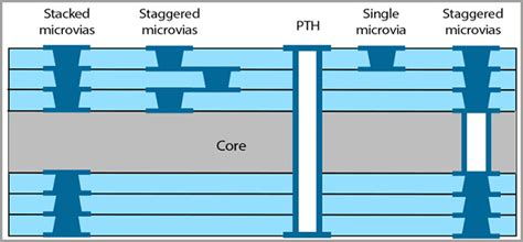
4. Micro Vias
Micro vias are small-diameter vias used in high-density interconnect (HDI) PCB designs. They are typically laser-drilled and have diameters ranging from 50 to 150 microns. Micro vias are used to create fine-pitch connections between layers, enabling the use of smaller components and higher component density. They are essential for advanced packaging technologies, such as chip-scale packaging (CSP) and ball grid array (BGA).
Characteristics of micro vias:
– Small-diameter vias (50 to 150 microns)
– Typically laser-drilled
– Used in HDI PCB designs
– Enable fine-pitch connections between layers
– Essential for advanced packaging technologies (CSP, BGA)
5. Stacked Vias
Stacked vias are a combination of multiple vias aligned vertically to create a continuous connection through multiple layers of the PCB. They are formed by drilling and plating the vias in a stacked configuration, with each via connecting two adjacent layers. Stacked vias are used to save board space and simplify routing in dense PCB designs.
Characteristics of stacked vias:
– Combination of multiple vias aligned vertically
– Create a continuous connection through multiple layers
– Formed by drilling and plating vias in a stacked configuration
– Used to save board space and simplify routing in dense PCB designs
6. Staggered Vias
Staggered vias are an alternative to stacked vias, where the vias are slightly offset from each other instead of being aligned vertically. This configuration helps reduce the stress on the PCB during the drilling and plating processes, minimizing the risk of manufacturing defects. Staggered vias also provide better signal integrity and reduced capacitance compared to stacked vias.
Characteristics of staggered vias:
– Vias are slightly offset from each other
– Alternative to stacked vias
– Reduce stress on the PCB during drilling and plating
– Minimize the risk of manufacturing defects
– Provide better signal integrity and reduced capacitance
7. Tented Vias
Tented vias are vias that are covered with soldermask on one or both sides of the PCB. The soldermask helps protect the via from oxidation, contamination, and short-circuiting. Tented vias are commonly used in PCB designs where the vias are not intended for component attachment or where additional insulation is required.
Characteristics of tented vias:
– Covered with soldermask on one or both sides of the PCB
– Protect vias from oxidation, contamination, and short-circuiting
– Used in PCB designs where vias are not intended for component attachment
– Provide additional insulation
8. Via-in-Pad
Via-in-pad is a technique where a via is placed directly within a component pad, allowing for a more compact PCB layout. This technique is particularly useful in designs with high component density or limited board space. Via-in-pad eliminates the need for additional traces between the component pad and the via, reducing the overall PCB Size and improving signal integrity.
Characteristics of via-in-pad:
– Via is placed directly within a component pad
– Allows for a more compact PCB layout
– Useful in designs with high component density or limited board space
– Eliminates the need for additional traces between the component pad and via
– Reduces overall PCB size and improves signal integrity

PCB Via Comparison Table
| Via Type | Description | Layers Connected | Drilling Method | Typical Diameter |
|---|---|---|---|---|
| Through-Hole | Drilled through entire PCB thickness | All layers | Mechanical drilling | > 200 microns |
| Blind | Starts from outer layer, terminates at inner layer | Outer to inner layer | Mechanical or laser drilling | 150-300 microns |
| Buried | Located entirely within inner layers | Inner layers only | Mechanical or laser drilling | 150-300 microns |
| Micro | Small-diameter vias for HDI designs | Outer to inner or inner to inner | Laser drilling | 50-150 microns |
| Stacked | Multiple vias aligned vertically | Multiple layers | Mechanical or laser drilling | Varies |
| Staggered | Vias slightly offset from each other | Multiple layers | Mechanical or laser drilling | Varies |
| Tented | Covered with soldermask on one or both sides | All layers | Mechanical or laser drilling | Varies |
| Via-in-Pad | Via placed directly within component pad | All layers | Mechanical or laser drilling | Varies |

Frequently Asked Questions (FAQ)
1. What is the purpose of vias in PCBs?
Vias in PCBs serve as conductive pathways that allow electrical signals to pass through different layers of the board. They enable efficient interconnections between components and layers, making it possible to create compact and complex circuit layouts.
2. What is the difference between blind and buried vias?
Blind vias start from an outer layer of the PCB and terminate at an inner layer, without passing through the entire board thickness. In contrast, buried vias are located entirely within the inner layers of the PCB, connecting two or more inner layers without reaching the outer surfaces of the board.
3. When should I use micro vias in my PCB design?
Micro vias are essential in high-density interconnect (HDI) PCB designs, where fine-pitch connections and smaller components are required. They enable higher component density and are crucial for advanced packaging technologies, such as chip-scale packaging (CSP) and ball grid array (BGA).
4. What are the advantages of using staggered vias over stacked vias?
Staggered vias offer several advantages over stacked vias. They help reduce stress on the PCB during the drilling and plating processes, minimizing the risk of manufacturing defects. Additionally, staggered vias provide better signal integrity and reduced capacitance compared to stacked vias.
5. How do via-in-pad techniques benefit PCB design?
Via-in-pad techniques allow for a more compact PCB layout by placing vias directly within component pads. This eliminates the need for additional traces between the component pad and the via, reducing the overall PCB size and improving signal integrity. Via-in-pad is particularly useful in designs with high component density or limited board space.

Conclusion
PCB vias are essential components in multi-layer PCB design, enabling efficient interconnections between layers and components. Understanding the different types of PCB vias, their characteristics, and their applications is crucial for creating robust and reliable circuit boards.
From through-hole vias for high-power applications to micro vias for HDI designs, each via type serves a specific purpose in PCB design. By selecting the appropriate via type and configuration, PCB designers can optimize board space, improve signal integrity, and ensure manufacturability.
As PCB technology continues to advance, staying informed about the latest via techniques and best practices is essential for designing cutting-edge electronic products. By leveraging the various types of PCB vias effectively, designers can create compact, high-performance, and cost-effective PCBs that meet the ever-growing demands of the electronics industry.