

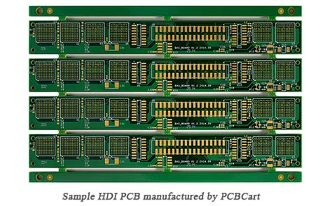
Introduction to HDI PCBs
High Density Interconnect (HDI) PCBs are advanced printed circuit boards that feature finer traces, smaller vias, and higher connection pad density compared to conventional PCBs. HDI technology enables the design and fabrication of compact, high-performance electronic devices with increased functionality and reliability.
The growing demand for miniaturization and enhanced performance in electronic products has driven the adoption of HDI PCBs across various industries, including consumer electronics, telecommunications, automotive, and aerospace.
Key Characteristics of HDI PCBs
- Higher density of interconnections
- Finer trace widths and spacing
- Smaller via diameters
- Thinner dielectric layers
- Increased number of layers
- Improved signal integrity and reduced signal losses
HDI PCB Structure
HDI PCBs consist of several layers of conductive copper traces and insulating dielectric materials. The structure of an HDI PCB is more complex than that of a standard PCB, featuring microvias, Buried vias, and blind vias to achieve higher interconnection density.
Microvias
Microvias are small, laser-drilled holes that connect the outer layers of an HDI PCB to the inner layers. These vias have a diameter of less than 150 microns and are typically filled with conductive material, such as copper, to establish electrical connections between layers.
Buried Vias
Buried vias are used to connect inner layers of an HDI PCB without extending to the outer layers. These vias are created by drilling and plating holes in the inner layers before laminating them together with other layers.
Blind Vias
Blind vias connect an outer layer to one or more inner layers without penetrating through the entire thickness of the PCB. Like microvias, blind vias are created using laser drilling and are filled with conductive material.
HDI PCB Stackup
The stackup of an HDI PCB refers to the arrangement of conductive and insulating layers. A typical HDI PCB stackup may include:
- Outer layers (top and bottom)
- Inner signal layers
- Power and ground planes
- Dielectric layers separating the conductive layers
The number of layers in an HDI PCB can vary depending on the complexity and requirements of the application. HDI PCBs often have 8 or more layers to accommodate the high density of interconnections.

HDI PCB Manufacturing Process
The manufacturing process for HDI PCBs involves several steps that differ from the fabrication of standard PCBs. These steps ensure the precise formation of fine traces, microvias, and other HDI features.
Design and Layout
The first step in HDI PCB manufacturing is the design and layout of the circuit. Engineers use specialized PCB design software to create the schematic and layout, taking into account the specific requirements of HDI technology, such as trace width, spacing, and via sizes.
Inner Layer Fabrication
The inner layers of an HDI PCB are fabricated by laminating a thin layer of copper foil onto a dielectric substrate. The copper foil is then patterned and etched to form the desired traces and pads.
Laser Drilling
Microvias and blind vias are created using laser drilling. A high-precision laser is used to drill small holes through the dielectric layers to establish connections between the inner and outer layers.
Plating and Filling
After laser drilling, the microvias and blind vias are plated with copper to create conductive paths. The vias are then filled with a conductive material, such as copper paste, to ensure reliable connections and prevent air gaps.
Lamination
The inner layers, along with the prepreg (pre-impregnated) dielectric material, are stacked and aligned in the desired sequence. The stack is then laminated under high pressure and temperature to bond the layers together.
Outer Layer Processing
The outer layers of the HDI PCB undergo a similar process of copper foil lamination, patterning, and etching to form the final traces and pads. Solder mask and silkscreen are applied to protect the circuitry and provide labeling.
Surface Finish
A surface finish, such as Immersion Gold (ENIG), Immersion Silver (IAg), or Organic Solderability Preservative (OSP), is applied to the exposed copper pads to prevent oxidation and enhance solderability.
Electrical Testing
The completed HDI PCB undergoes rigorous electrical testing to ensure the integrity of the connections and the functionality of the circuit. This may include automated optical inspection (AOI), flying probe testing, and functional testing.

Applications of HDI PCBs
HDI PCBs find applications in a wide range of industries and products where high performance, miniaturization, and reliability are essential. Some common applications include:
Consumer Electronics
- Smartphones
- Tablets
- Wearables
- Digital cameras
- Gaming consoles
Telecommunications
- 5G devices
- Routers and switches
- Fiber optic equipment
- Satellite communication systems
Automotive Electronics
- Advanced driver assistance systems (ADAS)
- In-vehicle infotainment systems
- Engine control units (ECUs)
- Sensors and actuators
Medical Devices
- Implantable devices
- Diagnostic equipment
- Wearable health monitors
- Surgical instruments
Aerospace and Defense
- Avionics systems
- Radar and surveillance equipment
- Satellite components
- Military communication devices

Advantages of HDI PCBs
HDI PCBs offer several advantages over conventional PCBs, making them the preferred choice for high-performance electronic applications:
Miniaturization
The higher density of interconnections and smaller components allowed by HDI technology enables the design of compact and lightweight electronic devices.
Improved Signal Integrity
The shorter signal paths and reduced layer count in HDI PCBs minimize signal losses and improve signal integrity, resulting in better overall performance and reliability.
Increased Functionality
HDI PCBs can accommodate a greater number of components and functions in a smaller footprint, enabling the development of feature-rich and complex electronic systems.
Cost Reduction
Although the initial fabrication costs of HDI PCBs may be higher than conventional PCBs, the overall system cost can be reduced through miniaturization, fewer components, and improved reliability.
Enhanced Thermal Management
The compact structure of HDI PCBs allows for better thermal management, as heat can be dissipated more efficiently through the use of thermal vias and advanced materials.
Challenges in HDI PCB Manufacturing
Despite the numerous advantages, HDI PCB manufacturing also presents some challenges that manufacturers must address:
Design Complexity
Designing HDI PCBs requires expertise in advanced PCB Layout techniques and a deep understanding of HDI technology. Designers must consider factors such as signal integrity, thermal management, and manufacturability.
Fabrication Precision
The smaller features and tighter tolerances in HDI PCBs demand high precision in the fabrication process. Manufacturers must invest in advanced equipment and maintain strict process controls to ensure consistent quality.
Material Selection
The choice of materials for HDI PCBs is critical to ensure reliable performance and manufacturability. Dielectric materials must have low loss tangents, while copper foils must be thin and smooth to enable fine trace formation.
Testing and Inspection
The high density of interconnections in HDI PCBs makes testing and inspection more challenging. Manufacturers must employ advanced testing techniques, such as 3D x-ray inspection and high-resolution automated optical inspection (AOI), to detect any defects or anomalies.
Cost Considerations
The advanced manufacturing processes and materials used in HDI PCBs can result in higher fabrication costs compared to standard PCBs. However, the overall system cost benefits often outweigh the initial investment.
Future Trends in HDI PCB Technology
As electronic devices continue to evolve and demand higher performance and smaller form factors, HDI PCB technology is expected to advance further. Some future trends in HDI PCBs include:
Increased Layer Count
HDI PCBs with 16 or more layers are becoming more common to accommodate the growing complexity of electronic systems.
Finer Feature Sizes
Trace widths and spacings are expected to decrease further, enabling even higher interconnection densities and more compact designs.
Advanced Materials
The development of new dielectric materials with lower loss tangents and higher thermal conductivity will enhance the performance and reliability of HDI PCBs.
Embedded Components
The integration of passive components, such as resistors and capacitors, directly into the PCB substrate will save space and improve signal integrity.
3D Printing
Additive manufacturing techniques, such as 3D printing, may be used to create complex HDI PCB structures and enable rapid prototyping.
Conclusion
HDI PCBs have revolutionized the electronics industry by enabling the design and fabrication of compact, high-performance devices. With their advanced structure and manufacturing processes, HDI PCBs offer numerous advantages, including miniaturization, improved signal integrity, increased functionality, and cost reduction.
As electronic systems continue to evolve and demand higher levels of performance and integration, HDI PCB technology will play a crucial role in driving innovation and meeting the challenges of the future.
Frequently Asked Questions (FAQ)
1. What is the difference between HDI PCBs and conventional PCBs?
HDI PCBs feature finer traces, smaller vias, and higher connection pad density compared to conventional PCBs. This enables the design of more compact and high-performance electronic devices.
2. What are microvias in HDI PCBs?
Microvias are small, laser-drilled holes that connect the outer layers of an HDI PCB to the inner layers. These vias have a diameter of less than 150 microns and are filled with conductive material to establish electrical connections between layers.
3. How many layers can an HDI PCB have?
The number of layers in an HDI PCB can vary depending on the complexity and requirements of the application. HDI PCBs often have 8 or more layers to accommodate the high density of interconnections.
4. What industries commonly use HDI PCBs?
HDI PCBs are used in various industries, including consumer electronics, telecommunications, automotive, medical devices, aerospace, and defense, where high performance, miniaturization, and reliability are essential.
5. What are the main challenges in HDI PCB manufacturing?
The main challenges in HDI PCB manufacturing include design complexity, fabrication precision, material selection, testing and inspection, and cost considerations. Manufacturers must address these challenges to ensure the consistent quality and reliability of HDI PCBs.