

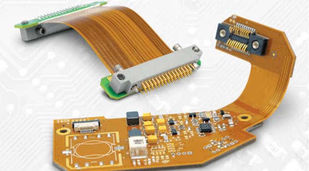
Introduction to Flex PCBs
A flex PCB, also known as a flexible printed circuit board, is a type of PCB that is made of flexible materials and can bend and flex. Flex PCBs have become increasingly popular in recent years due to their many advantages over traditional rigid PCBs. Some key benefits of flex PCBs include:
- Ability to bend and flex: This allows flex PCBs to fit into tight or moving spaces that rigid PCBs cannot. Very useful in compact electronics and wearable devices.
- Highly customizable: Flex PCBs can be fabricated with different types of flexible materials to meet specific mechanical or electrical needs.
- Better signal integrity: The flexibility allows traces to stay in closer contact during flexing, which maintains signal quality.
- More durable: Flex PCBs are resistant to vibrations and impacts that could damage rigid boards.
- Lighter weight: Without a rigid board substrate, flex PCBs are lighter than rigid PCBs. Important for portable electronics.
- Easier assembly: Components can be assembled directly onto flex PCBs, eliminating the need to attach a separate rigid PCB.
When to Use 4 Layer Flex PCBs
The number of layers in a flex PCB refers to the number of conductive copper layers separated by flexible dielectric material. While single or double layered flex boards are common, some applications require more layers.
4 layer flex PCBs offer some key advantages over fewer-layered boards:
- Increased circuit complexity: A 4 layer board provides more space for routing complex circuit designs. This added routing space allows for more components and capabilities.
- Better impedance control: With a ground layer and power layer, 4 layer boards offer better control over electrical impedance for high speed signals.
- Higher circuit density: More layers allow components and traces to be tightly packed, increasing overall circuit density.
- Improved power delivery: Separate power and ground layers improve voltage regulation for power hungry components.
- Enhanced EMI shielding: Ground layers provide shielding from electromagnetic interference.
Some examples of applications where a 4 layer flex PCB would be suitable:
- Complex wearable devices.
- Multilayer flex-rigid PCBs with both flex and rigid sections.
- High density interconnects between multiple PCBs.
- Flexible circuits with components on multiple sides.
- High speed circuits for data communications.
For simpler low-density circuits, 2 layer boards remain the most cost effective option. But when design constraints demand it, a 4 layer flex PCB provides important benefits.
4 Layer Flex PCB Design Considerations
Designing a 4 layer flex PCB comes with some important considerations to take into account compared to simpler 2 layer boards. Here are some key guidelines for 4 layer flex PCB layout.
Layer Stackup
The layer stackup defines the sequence of conductive copper and dielectric layers in the flex PCB. For 4 layer boards, there are two common stackup configurations:
4 Layer Stackup #1
- Layer 1 (Top): Signal Layer
- Layer 2 (Internal 1): Ground Layer
- Layer 3 (Internal 2): Power Layer
- Layer 4 (Bottom): Signal Layer
4 Layer Stackup #2
- Layer 1 (Top): Signal Layer
- Layer 2 (Internal 1): Signal Layer
- Layer 3 (Internal 2): Ground/Power Plane
- Layer 4 (Bottom): Signal Layer
The first option provides a full ground/power plane pair for improved impedance control, shielding, and power delivery. But it splits the signal routing on two layers.
The second option allows all signal routing on outer layers but has no continuous power plane. It offers higher density but less optimal electrical performance.
Dielectric Material
The dielectric material separates the copper layers. Typical options for 4 layer flex PCBs include:
- Polyimide: High flexibility and temperature resistance but more expensive. Used in dynamic flexing applications.
- Polyester: Lower cost but has less flexible properties. Used for static flex applications.
- Fluoropolymer: Low loss material suitable for high frequency boards. More expensive.
- Adhesive layers: Bonds multilayer constructions. Can be acrylic, epoxy, or thermoplastic based.
The dielectric materials impact flex life, impedance, loss, and other electrical properties.
Trace Width and Spacing
Narrower traces and spacing are possible on flex PCBs vs rigid boards. Here are typical guidelines:
- Minimum trace width: 0.1mm (4 mils)
- Minimum spacing: 0.1mm (4 mils)
Thinner and tightly spaced traces should be used cautiously in dynamic flexing applications as the cumulative stresses can deteriorate traces over time.
Bending Radius
Sharply bending flex PCBs repeatedly can cause metal traces to crack. The minimum bend radius depends on the stackup:
- 2 layer boards: 0.125 x PCB thickness
- 4 layer boards: 0.25 x PCB thickness
The more layers, the larger bend radius required. Flex life also depends on materials used.
Stiffeners
Strategically placed stiffeners made of rigid material can be used to control areas of flex PCBs that require stability for mounting components or connectors.
Flex-to-Rigid Transition
A rigid section may be needed for component mounting or connectors. A controlled gradual transition between the flex and rigid areas is important to avoid excessive stresses.
CAD Tools
Specialized flex PCB design software tools are recommended for 4 layer boards to assist with flex stackups, bend radius, layer fanouts, and documentation.
Manufacturing 4 Layer Flex PCBs
Producing a reliable 4 layer flex board requires expertise in the nuances of flex PCB fabrication. Here is an overview of the manufacturing process.
Laminating
The dielectric and adhesive layers are precisely laminated together under heat and pressure to form the multilayer construction. Careful process control prevents entrapped air bubbles.
Etching
Photolithographic printing transfers the circuit pattern onto the copper layers. Etching then removes unwanted copper to leave the desired traces and features.
Coverlay Application
A thin coverlay layer is laminated onto the top and bottom sides to protect the delicate traces. Coverlay cutouts expose solder pads and areas for components and vias.
Via Formation
Mechanical and laser drilling create vias through the dielectric layers to interconnect traces between layers. Plating makes the vias conductive.
Solder Mask
The solder mask layer coats the board to prevent solder from bridging between traces. Openings in the mask define solderable areas.
Finishing
Final finishes like ENIG (electroless nickel immersion gold) can be applied to protect copper traces from oxidation and improve solderability.
Testing
Electrical testing validates the boards meet circuit requirements. Automated optical inspection checks for defects and quality assurance.
Singulation
Individual PCB sections are cut or routed from the larger manufactured panel.
Producing advanced multilayer flex PCBs requires an expert manufacturer with the knowledge and process capabilities to meet tight tolerances and ensure reliability.
FQA
What are some advantages of 4 layer flex PCBs?
Some main advantages of 4 layer flex PCBs are increased routing space for complex circuits, better impedance control for high speeds, higher circuit density, improved power delivery, and enhanced EMI shielding from ground planes.
What are some typical applications of 4 layer flex PCBs?
Typical applications that benefit from 4 layer flex PCB technology include complex wearable devices, multilayer flex-rigid boards, high density interconnects, flexible circuits with components on multiple sides, and high speed data communications.
What are some key 4 layer flex PCB design considerations?
Important design considerations include: selecting the optimal layer stackup for the application, managing trace widths/spacing, controlling flex bend radius, incorporating stiffeners, planning proper layer transitions, and using specialized CAD tools.
What is the minimum bend radius for a 4 layer flex PCB?
The minimum bend radius for a 4 layer flex board is typically 0.25 x the total PCB thickness. So a 4 layer PCB with a total thickness of 1mm would have a minimum bend radius of 0.25mm.
What are some key manufacturing processes for 4 layer flex PCBs?
Precision laminating, photolithographic etching, coverlay application, via formation, solder mask coating, surface finishing, electrical testing, and singulation are some of the critical manufacturing processes required to produce reliable 4 layer flex PCBs.