

What is the difference between PCB assembly and PCB manufacturing?
Introduction
Printed circuit boards (PCBs) form the core of electronics hardware, providing the foundation for mounting and interconnecting electronic components.
There are two key parts of realizing a functional PCB –
1. PCB Manufacturing: Producing the bare printed circuit board
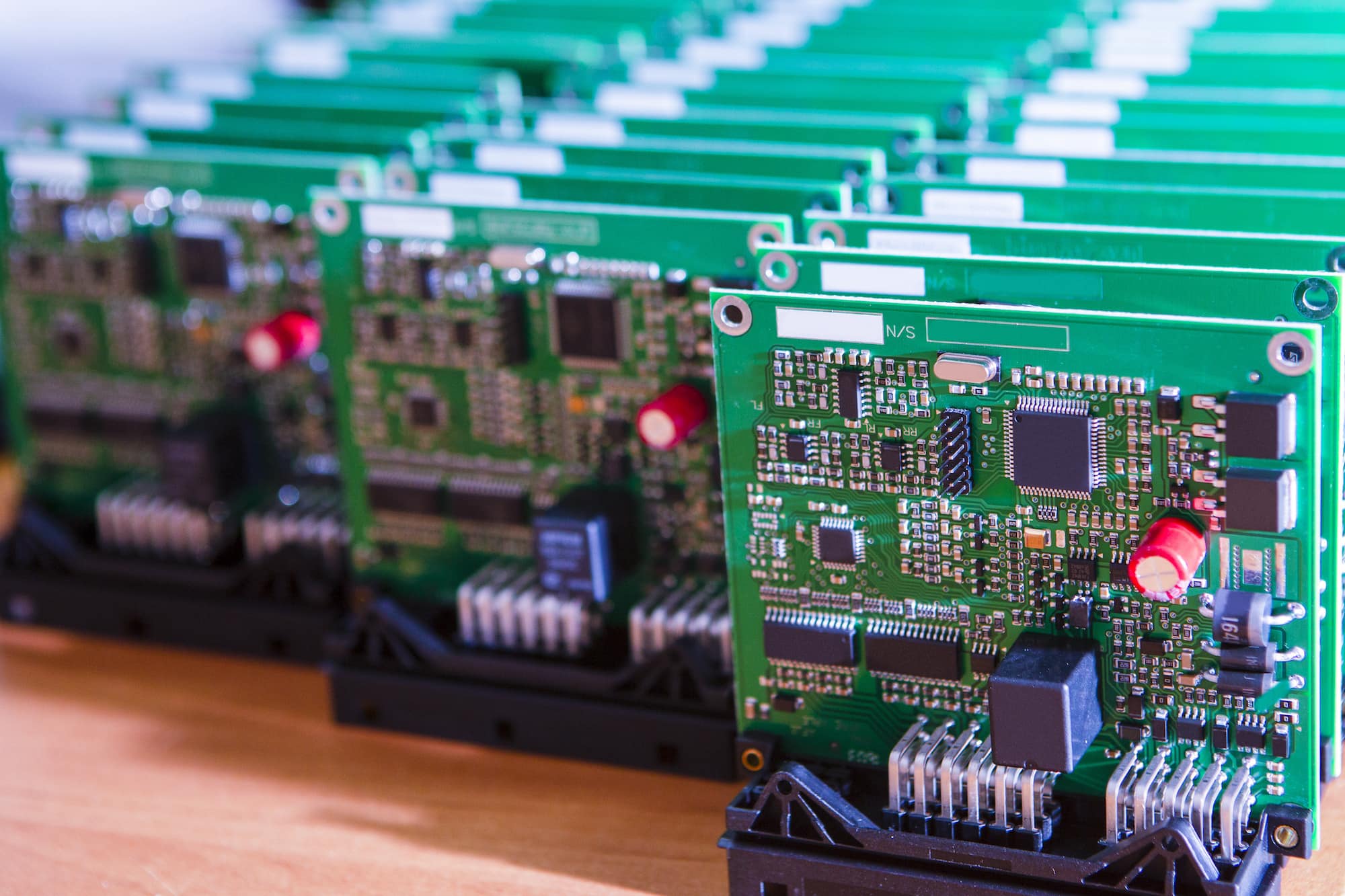
2. PCB Assembly: Stuffing components onto the fabricated bare boards
Understanding the exact distinction between these two terms is important for appropriate planning, costing, quality control and interactions with vendors during electronics production cycles.
PCB Manufacturing
PCB manufacturing refers to the processes involved in fabricating the raw printed circuit board (PCB) without any components populated on it.
It converts design data from CAD layout tools into actual physical boards with conductive copper traces, pads, vias, laser drilled holes and other features that provide electrical connectivity.
The bare boards emerge from PCB factories containing just the printed wiring substrate ready for component assembly in later stages.
Stages of PCB Fabrication
The major manufacturing steps to fabricate a bare PCB are:
1. Board Preparation
- Generate manufacturing CAM files from PCB design data
- Clean substrate panel surfaces thoroughly
2. Photolithography
- Laminate photoresist layer onto copper clad dielectric substrates
- Expose selective areas using special photomasks
- Develop resist to form patterned openings on copper foil
3. Copper Etching
- Etch away unwanted copper in areas unprotected by resist layer
- Strip off remaining photoresist after etching
4. Hole Drilling
- Drill holes for component pins and conductive vias
5. Hole Plating
- Plate conductive copper over wall of drilled holes
6. Soldermask Application
- Screen print epoxy resin layer with openings over bonding pads
7. Legend Printing
- Screen print markup layer for part outlines, markings etc.
8. Surface Finish
- Coat exposed copper with solder, gold, tin or other protective finish
9. Panel Scoring/Depaneling
- Score lines or routed edges to facilitate board separation
10. Electrical Testing
- Validate layer-to-layer connections electrically
11. Visual Inspection
- Scan for defects & measure tolerance conformance
This sequence of steps results in fabricated PCBs ready for component assembly. The combination of processes used depends on the product design requirements.
PCB Fabrication Types
There are a variety of PCB base material types and fabrication processes tailored to suit applications –
| PCB Type | Build Process | Volume | Cost |
|---|---|---|---|
| Single Sided | Most basic, Cu on 1 side only | Low | Cheapest |
| Double Sided | Cu on both sides | Medium | Low |
| Multilayer | Complex process, 30+ layers possible | High | High |
| Metal Core PCB | Base is metal plate for thermal dissipation | Low | Expensive |
| Flex PCB | Flexible substrate material | Medium | Medium |
| Rigid-Flex | Combination of flex and rigid sections | Low | High |
| HDI PCB | Fine features, microvias, tighter spacing | High | Very High |
PCB Specification
Key requirements to be detailed for bare board fabrication based on product needs are:
- Layer count
- Stackup – core thickness, copper weights
- Material types
- Line width/Spacing
- Hole sizes – thru hole, buried, blind vias
- Pad dimensions
- Surface finish – HASL, ENIG, Imm Ag, OSP
- Copper thickness
- Final panel dimensions
- Soldermask color
- Silkscreen print text
- Impedance control specs
- Testing procedures
- IPC standards class
- Special fabrication process instructions
- Gerber, drill, netlist, drawings and other CAM files
By providing comprehensive manufacturing specifications, the PCB fabrication vendor has all the necessary processing rules and build instructions to produce the bare printed wiring board accurately.
PCB Assembly
PCB assembly, also called PCA (Printed Circuit Assembly), involves soldering and connecting electronic components onto the fabricated PCB to realize the full electronic circuit or system.
It is transforming bare printed circuit boards into functional boards by mounting ICs, resistors, capacitors, connectors and other parts onto the boards by means of soldering or socketing. This process is thus also referred to as board stuffing, board population, or through-hole/SMT assembly.
Stages of Manual PCB Assembly
For low volume board stuffing done manually, the assembly sequence is roughly:
- Parts Arranging – Get all parts/ingredients ready
- Solder Paste Dispensing – Put solder paste on PCB pads
- Component Placement – Position parts on the board
- Reflow Soldering – Heat up to fuse parts to pads
- Inspection – Verify all parts mounted properly
- Testing & Rework – Confirm board works electrically; Fix issues
- Conformal Coating – Protect assembled boards against environmental damage
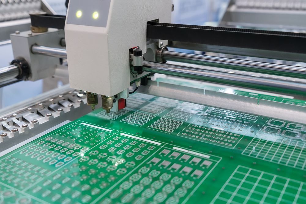
As production volumes scale for complex boards, specialized automated SMT (Surface Mount Technology) assembly machines and optimized processes take over.
High Volume SMT Assembly
Mass production PCB assembly with SMT components is done using precise pick-and-place machines and reflow ovens. Steps include:
- Solder Paste Stenciling – Solder paste printed on pads
- High-speed Component Placement – Machine picks parts from tapes and accurately mounts them onto paste
- Reflow Soldering – Infrared/convection oven solders parts to board
- Inspection – Optical checking of placements
- Testing – Validating of key parameters
- Board Wash – Cleaning flux residues
- Conformal Coating – Protective material against environmental damage
- Packaging – ESD bags/boxes
The assembly equipment and factory floor space requirements for SMT based PCB assembly is high. Hence volume requirements need to justify establishing these production lines.
Core Differences Between PCB Fabrication vs Assembly
| Parameter | PCB Fabrication | PCB Assembly |
|---|---|---|
| Stage | Early, After Design Complete | Later, End of HW Development Cycle |
| Process | Complex base board fabrication | Mounting components by soldering |
| Input | Gerber, CAD and CAM files | Bare boards and loose components |
| Expertise | Material science, photolithography, plating, etching | Soldering processes, ESD control |
| Capital Equipment | Film printers, etching machines, plating lines, testers | Pick and place machines, reflow ovens, wash systems |
| Scale | Batch processing many panels in parallel | Sequential board-by-board population |
| Lead Time | 2-3 weeks typically | 1 week typically |
| Cost Structure | High NRE/tooling, lower piece cost | Lower NRE, higher piece cost |
| Role Specialization | PCB Fabricators / Board Houses | Contract Manufacturers / EMS partners |
Understanding the clear demarcation across these facets helps assign responsibility areas appropriately between supply chain partners during electronics hardware manufacturing.
Global Ecosystem
There exist well defined ecosystems and specializations across vendors focused exclusively on PCB fabrication vs assembly.
PCB Manufacturing Industry
There are about 3000+ PCB fabrication facilities worldwide producing over $60 billion worth of bare boards per year. The geographic breakup is:
| Region | Market Share |
|---|---|
| China | >50% boards made |
| Asia outside China | ~30% |
| Americas | ~13% |
| Europe | <5% |
Leading bare board manufacturers by revenue include – Compeq, AT&S Austria, TTM Technologies, Tripod, Unimicron, Ibiden etc.
Chinese vendors dominate high volume cost driven boards while advanced HDI and packaging boards are made in Taiwan, Korea and Japan. Specialized RF boards are produced in North America and Europe.
PCB Assembly Industry
Top PCB assemblers worldwide based on revenue are –
| Company | Location | Revenue |
|---|---|---|
| Advanced Assembly | USA | $24m |
| Valor | USA | $50m |
| SMTC | Canada | $418m |
| Flex | Singapore | $500m |
| Jabil | USA | $25.3b |
| Sanmina | USA | $27.5b |
| Foxconn | Taiwan | $40b |
| Pegatron | Taiwan | $43b |
| Compal | Taiwan | $28b |
High mix variability and quick ramp up capability has enabled EMS partners to dominate mid/high volume PCB assembly for regional as well as global customers.
PCB Fabrication vs Assembly – Comparison FAQs
Q1. Should PCB fabrication data be shared with assemblers?
Manufacturing notes and stackups help assemblers adapt processes, but intellectual property should be protected by not sharing original CAD data.
Q2. How to select PCB assembly partners for prototypes vs production?
Use local assemblers for fast-turn low volume prototypes. Transfer to offshore high volume partners for production ramps with process capability assessment.
Q3. What process validations are required while outsourcing fabrication and assembly?
For fabrication, ICT/FCT testing confirms electrical connectivity. For assembly, visual inspection and functional testing ensures reliable working boards.
Q4. How to reduce costs across PCB fabrication, components and assembly?
Standardizing designs on qualified processes yields cost benefits. Value engineering through component engineering, panel utilization improvement and test optimization also help.
Q5. What are key considerations for quality management during fab and assembly?
Certifications like ISO, IATF 16949 demonstrate vendor process capabilities. Product-specific test coverage validation ensures high yields and reliability. IP protection protocols also safeguard design data confidentiality.
Conclusion
In summary – PCB fabrication involves manufacturing the raw printed circuit boards from base dielectric materials through complex photolithography, plating and etching processes. The resultant bare boards shipped from board houses then undergo component assembly and soldering by contract manufacturers to create loaded functional boards ready for system integration.
Keeping this distinction clear between the roles of the PCB fabrication and assembly supply chain partners facilitates efficient manufacturing handoffs during the electronics product development cycle.