

Introduction
A printed circuit board (PCB) is the foundation of any electronic product. It provides the mechanical structure and electrical connections between components. Rigid PCBs were once the only option, but flexible PCBs (FPCBs) are now widely used due to their ability to bend and flex. Multilayer FPCBs take this a step further by stacking multiple conductive layers with insulation between them. This allows for increased component density and more complex circuitry in a small space.
In this guide, we will explore the key aspects of multilayer flexible PCB design, materials, manufacturing, and applications. With the right knowledge, multilayer flex circuits can be readily designed and produced.
What are Multilayer Flexible PCBs?
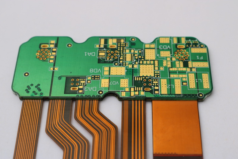
A multilayer FPCB contains two or more conductive copper layers separated by flexible dielectric material. The layers are bonded together under heat and pressure. conductive layers are etched to form traces, pads, vias, and other features. Flexible boards can have 2 to 12 or more layers, with 2 to 6 being most common.
Compared to double-sided FPCBs, multilayer flex offers:
- More space for traces and components
- Ability to route signals on inner layers
- Dense, complex circuitry
- Embedded passives and actives
- Shielding from EMI/RFI
Some key terms related to multilayer FPCBs:
- Coverlay: A flexible dielectric laminated over the top conductive layer for insulation and protection.
- Via: A plated through hole that connects traces between layers.
- Buried Via: A via that connects inner layer traces without going to the outer layers.
- Blind Via: A via that connects only between adjacent layers.
- Fill: Copper plating within a via for conductivity.
- Annular Ring: The copper pad around a via opening.
Multilayer Flex Materials
Multilayer flex circuits use specialized flexible materials that can withstand repeated bending. Typical materials include:
- Polyimide (PI): A high-performance polymer that can tolerate continuous flexing. Common types are Kapton from Dupont and Apical from Kaneka.
- Polyester (PET): A more economical option. Often used for less demanding applications.
- Coverlay: Liquid crystal polymer (LCP) or acrylic adhesive offer robust protection.
- Bonding Film: Acrylic or modified epoxy adhesive films bond the layers together.
- Solder Mask: Liquid photoimageable solder mask (LPISM) coats the traces for protection and insulation.
The materials must be properly adhered, have compatible coefficients of thermal expansion, and retain flexibility. The process and materials are engineered to avoid cracking or delamination during flexing.
Design Considerations
Designing a multilayer FPCB requires special considerations for the flexible material and multi-layer stackup. Here are some key guidelines:
- Trace width and spacing: Follow recommended widths and clearances based on circuit current, voltage, and flexing requirements.
- Stackup: Ensure adequate dielectric thickness between layers to prevent shorts. Allow for thickness of bonding films.
- Bend radius: Avoid tight folds and enable sufficient bend radius for the stackup. Limit fold locations.
- Vias: Use buried and blind vias to optimize routing between layers. Allow for adequate annular rings.
- Stiffeners: Add stiffener materials in areas without folding to provide support. Prevent connections from cracking.
- Adhesives: Use flex-compatible adhesives for components. Avoid rigid adhesives that inhibit bending.
- Reinforcement: Consider adding reinforcement material for high-wear folding areas.
Following industry design rules and flex PCB guidelines will ensure the board can withstand the mechanical and electrical demands.
Manufacturing Process
Producing multilayer flex circuits requires specialized manufacturing equipment and processes tailored for flexible materials. Here is a general sequence:
- Materials Prep: The flexible dielectric and adhesive bonding films are prepared. Coverlay, soldermask, and other coatings are applied to materials as needed.
- Layer Imaging: Using photolithographic processes, the conductive copper foils are imaged and etched to form the traces, pads, and features on each layer.
- Layer Alignment: The etched flex layers are precisely aligned and stacked in the proper sequence.
- Layer Bonding: The layers are adhered together through a high pressure lamination process.
- Via Formation: Mechanical or laser drilling forms the through holes for vias. The vias are plated to connect traces between layers.
- Soldermask and Finishing: Soldermask, markings, and other finishing steps are completed. The boards may be electrically tested.
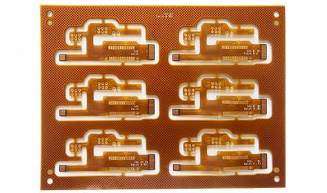
- Singulation: Individual PCBs are cut from the panelized boards.
- Quality Inspection: 100% inspection ensures quality and reliability. Automated optical inspection (AOI) is often used.
The combination of specialized materials, precision alignment, and advanced manufacturing techniques makes production of multilayer flex circuits complex compared to rigid PCBs.
Multilayer Flex Applications
Some uses and industries that benefit from multilayer flexible PCB technology:
- Wearable devices: Fitness bands, smart watches, health monitors.
- Medical: Hearing aids, implants, probes.
- Automotive: Lighting, sensors, control panels, EV circuitry.
- Consumer electronics: Cell phones, cameras, displays.
- Defense: Missiles, radars, aerospace avionics.
- Industrial: Robotics, machine controls, instrumentation.
For many products, multilayer flex provides the ideal combination of small size, light weight, ruggedness, and complex connectivity.
Pros and Cons of Multilayer Flex Circuits
Pros:
- Compact size and shape versatility
- Ability to embed components
- Dynamic and repeated flexing capability
- Complex circuitry with dense traces
- Shielding from EMI/RFI
- Reliability and durability
- Light weight compared to rigid boards
Cons:
- Generally higher cost than rigid PCBs
- Limited number of layers compared to rigid boards
- Tight design rules require expertise
- More complex manufacturing process
- Can require special connectors
The Future of Multilayer Flex
Multilayer FPCB technology will continue advancing to enable smarter and more dynamic products:
- More layers: Expect to see mainstream boards progressing beyond 6 layers.
- Thinner dielectrics: Allowing tighter layer stacks and more compact boards.
- Improved flex life: Through new materials and coatings.
- Higher density integration: With fine features below 25 microns.
- Advanced applications: Such as flexible electronics, rollable displays, biosensors, and medical devices.
With their unique combination of small size, light weight, and rugged flexibility, multilayer flex circuits will remain an important PCB technology moving forward.
Frequently Asked Questions
1. What are the typical dielectric materials used in multilayer flex boards?
The most common dielectric materials are polyimide (PI) films such as Kapton or Apical. Other options include polyester (PET), liquid crystal polymer (LCP), and various adhesive films. The materials are selected based on flexibility, bondability, thermal performance, and cost considerations.
2. What are some typical layer counts for multilayer flex circuits?
While 2 layer flex boards are common, multilayer flex PCBs often have 4, 6 or 8 conductive layers. High-density boards may go up to 10 or 12 layers, while complex circuits can have 20+ layers. The number of layers depends on the interconnectivity required balanced with cost and manufacturability.
3. How are components mounted on multilayer flex boards?
SMT components are commonly used on multilayer flex. Adhesives help secure components and accommodate flexing. Through-hole components with compliant leads can also be used. Chips can sometimes be embedded between layers. Specific pad sizes, pitch, and clearances are followed for flex assemblies.
4. How small can the traces and spacing be on multilayer flex PCBs?
The lines and spaces depend on the fabrication capabilities, currently reaching about 25-50 microns (1-2 mils). This allows a high level of miniaturization. Finer features are expected in the future as flex PCB technology progresses.
5. What are some methods used to interconnect layers on multilayer flex boards?
Plated through hole vias are the primary method. Blind and buried vias optimize connections between inner layers. Microvias under 0.15mm are possible. Alternatives like conductive adhesives or direct layer contact through windows are also used in some cases.