

ntroduction
Flexible printed circuit boards (flex PCBs) have become increasingly popular in recent years due to the growing demand for smaller and more flexible electronics. Flex PCBs allow circuits to bend and flex to fit into tight or moving spaces. They are most commonly used in consumer electronics, medical devices, aerospace applications, and more. Flex PCB fabrication involves specialized materials and processes to create a thin, bendable circuit board. This article will provide a comprehensive guide on flex PCB fabrication covering the following topics:
- Flex PCB Materials
- Design and Layout
- Manufacturing Processes
- Photolithography
- Etching
- Die Cutting
- Lamination
- Final Testing
- Advantages and Disadvantages
- Cost Analysis
- FQA
Understanding the intricacies of flex PCB fabrication will allow you to properly design, source, and integrate flex circuits into your products.
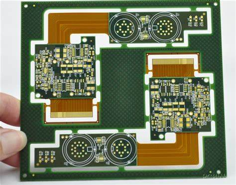
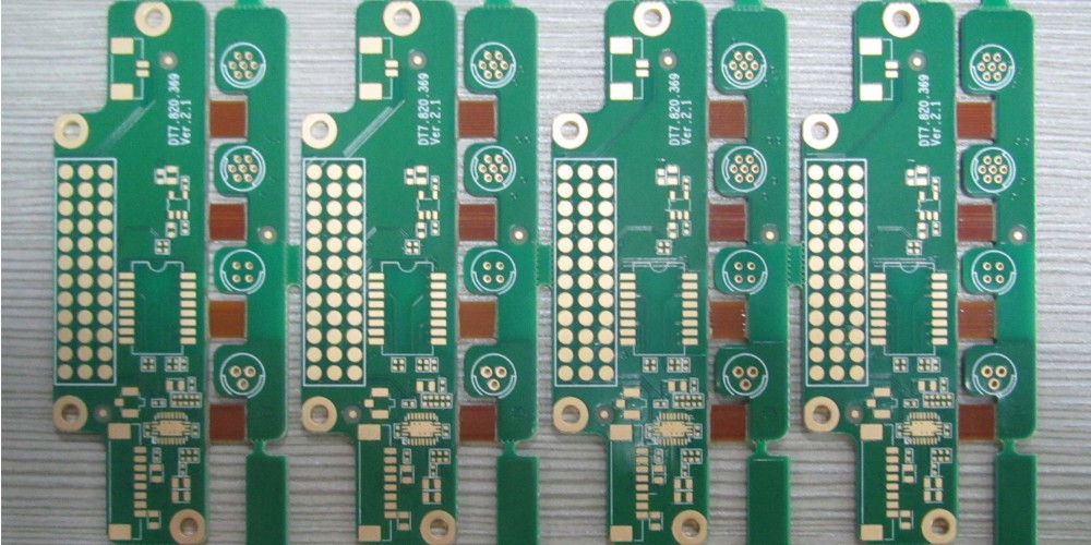
Flex PCB Materials
Flex PCBs are fabricated from extremely thin, flexible base materials that are able to withstand bending and repeated motion. The most common base materials include:
- Polyimide (PI) – Most popular flex PCB material. Polyimide offers high heat resistance, chemical resistance, and mechanical strength. Commonly known as Kapton. Thickness range: 12.5-100μm.
- Polyester (PET) – More economical alternative to polyimide. Polyester has moderate flexibility and temperature resistance. Thickness range: 12.5-125μm.
- Polyethylene Naphthalate (PEN) – High temperature resistance up to 200°C. Used for applications with extreme bending. Thickness range: 12.5-125μm.
Other materials like polyvinyl chloride (PVC) and polyethylene terephthalate (PET) are also sometimes used as base materials. The base material thickness depends on the amount of flexibility required. Thinner bases allow for tighter bends. Common copper foil thickness ranges from 12-35μm. Flex PCBs generally use rolled annealed copper which has enhanced flexibility compared to electro-deposited (ED) copper foil.
Design and Layout Considerations
Designing a flex PCB requires special considerations regarding the circuit layout, component selection, and board shape.
Here are some key flex PCB design guidelines:
- Allow for expansions/contractions – Use larger trace widths and clearances to account for material expansion and contractions during bending. This helps prevent cracked traces.
- Avoid 90° angles – Angles concentrate stress. Use rounded corners instead with a minimum radius of 3X the material thickness.
- Minimize components – Limit component quantity on the flexing areas of the PCB. Adhesives can reduce flexibility.
- Reinforce components – Use stitching vias around component pads or underfill adhesive to reinforce component connections.
- Mind layer stackup – Alternate the placement of copper layers symmetrically around the base material to avoid distortion.
- Simplify board outline – Avoid complex board shapes and cutouts to reduce stress points.
Following these guidelines will optimize the PCB layout for flexing applications and help avoid failures.
Flex PCB Fabrication Process
Fabricating a flex PCB involves specialized processes and equipment to handle the thin, flexible materials. Here is an overview of the typical manufacturing workflow:
1. Photolithography
A photoresist (photosensitive polymer) is laminated onto the copper-clad base material. The board then goes through an imaging process which selectively exposes areas of the photoresist according to the circuit pattern design.
2. Etching
The exposed photoresist is dissolved away, revealing bare copper for etching. The boards are sprayed with an etchant chemical to remove the unwanted copper leaving only the desired circuit traces.
3. Die Cutting
Once the photoresist is stripped away, the individual PCBs are mechanically cut from the panel using a precision die cutting machine. This separates the boards from the panelized sheet.
4. Lamination
Several layers of etched flexible circuits can be bonded using adhesive films to create multilayer flex PCBs. Multilayer boards provide advantages like allowing crossing traces between layers. Heat and pressure melt the adhesive layers bonding the materials.
5. Final Testing
Finished boards undergo electrical testing (ICT, flying probe) to verify all connections and functionality meet specifications. Automated optical inspection (AOI) also checks for any physical defects or irregularities.
Advantages and Disadvantages of Flex PCBs
Here are some key benefits and limitations of using flex PCB technology:
Advantages:
- Extremely compact and thin profile – Enables smaller electronics
- Can conform to bend and move – Fits dynamic applications
- Highly durable and reliable – Built to withstand repeated flexing
- Lightweight – Reduces product weight over rigid PCBs
- Design freedom – Flexible shape allows industrial design creativity
Disadvantages:
- Limited in component area – Smaller components must be used
- Increased complexity – Requires special materials and design considerations
- Higher cost – Flex PCB fabrication has specialized processes
Flex PCB Cost Analysis
The costs of flex PCBs are driven by several factors:
- Base Material – Polyimide is standard and cost effective. Polyester is cheaper. PEN is more expensive. Thinner material reduces cost.
- Layer Count – Single layer is lowest cost. 2-6 layers are common. More than 8 requires additional lamination steps.
- Board Size – An inverse relationship between size and cost per unit area due to material usage. Panel utilization optimization helps reduce cost.
- Quantity – Higher volumes distribute setup costs lowering cost per board. Prototyping has high costs.
- Flexibility – More bendable designs require thinner flexible materials that increase costs.
- Testing/Certifications – Rigorous testing like IPC Class 3, UL certification, etc. add cost if required.
As a rough estimate, simple 2-4 layer flex PCBs in small volumes can range from $200-$1000 per design. High volume production can drive this down significantly. Consulting with a flex PCB manufacturer is recommended to obtain accurate pricing.
FQA
Here are some frequently asked questions about flex PCB fabrication:
Q: What are some typical applications of flex PCBs?
A: Flex PCBs are widely used in electronics that require dynamic bending and flexing like wearables, medical devices, robotics, automotive, aerospace, and consumer electronics. Common examples include wearable health trackers, hearing aids, cameras, and display flex cables.
Q: Can components be mounted directly on flex PCBs?
A: Yes, but the types of components are limited. Common component types include chip resistors and capacitors, LEDs, bare die, and extremely small packaged ICs. Flexible adhesives are used for mounting. Bulky, rigid components are not recommended in flexing areas.
Q: How small can flex PCB traces and spaces be fabricated?
A: The fabrication limits are driven by the photolithography process. Typical trace/space is around 100um (4 mils), while some flex PCB fabs can achieve 50um (2 mil) traces. Finer geometries are possibly with laser direct imaging (LDI).
Q: How many times can flex PCBs be flexed before failure?
A: Many flex PCBs can withstand over 1 million dynamic flex cycles. The flex life depends on several factors like material type, bend radius, and layout. Proper design is critical for maximizing flex capability.
Q: What types of testing are performed on flex PCBs?
A: Flex PCBs typically undergo electrical testing like flying probe, along with visual inspection. IPC Class 3 flex tests involve flexural endurance testing ensure the design meets requirements through the full motion cycle. Test coupons may also be used.
Conclusion
Flex PCB fabrication enables innovative, reliable circuit designs that can bend and move with your application requirements. The specialized materials, layout considerations, and manufacturing processes required for quality flex circuits were covered in this guide. With careful design and by leveraging a knowledgeable flex PCB manufacturer, you can fully capitalize on the benefits of flexible printed circuit boards in your electronics projects. Please contact us if you have any other questions!