


What is flex rigid PCB?
Introduction to flex rigid PCBs
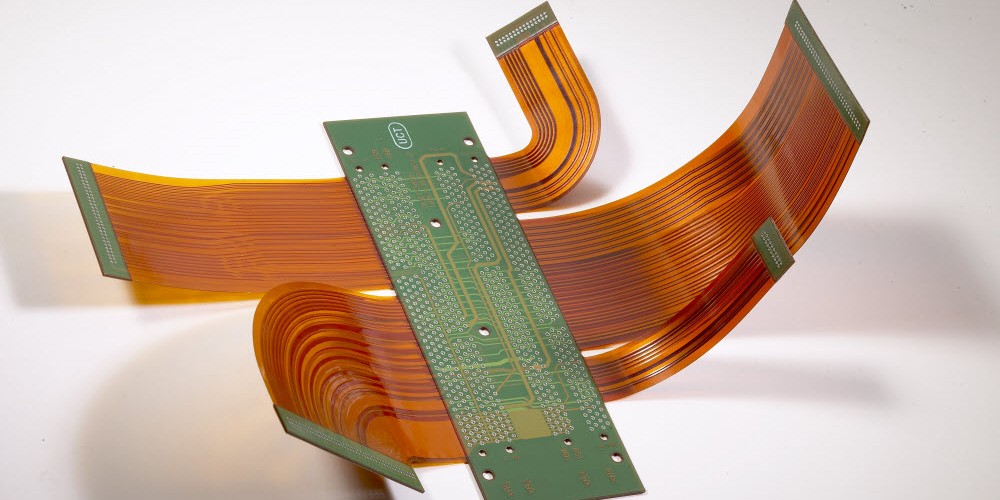
A flex rigid printed circuit board (PCB) is a specialized type of circuit board that combines rigid and flexible substrates to create a single PCB. These hybrid PCBs provide mechanical support while also allowing dynamic flexing and bending in certain areas of the board.
Flex rigid PCBs provide several key advantages:
- Flexibility – Flexible sections of the PCB can bend and twist to accommodate mechanical systems and complex form factors, while retaining connectivity.
- Reliability – Rigid sections provide structural stability for mounted components and traces.
- Weight and space savings – Consolidating rigid and flex PCBs into a single design saves weight and space compared to using two separate boards.
- Design freedom – Allows for more creative and complex PCB and product designs that can fit and operate in tight spaces.
With these hybrid properties, flex rigid PCBs are ideal where dynamic mechanical flexibility and strength are both required in the application.
Rigid Sections vs Flexible Sections
The rigid sections of a flex rigid PCB provide mechanical stability while the flexible sections allow for dynamic contours and shapes.
Rigid Substrates
The rigid sections are typically made from standard glass reinforced epoxy laminate materials such as FR-4. These provide structural stability for mounted components and to maintain form factor tolerance across the rigid sections.
They also provide thermal mass and reduce thermal expansion and contraction, helping protect sensitive components. And the fiberglass construction gives enhanced Z-axis stability between copper layers, protecting trace impedance.
Flexible Substrates
The flexible layers are composed of polyimide films such as KaptonTM or flex-grade epoxies reinforced with fabric, allowing them to freely bend and twist repeatedly over a long lifetime.
Flexible layers have thickness between 25-100μm while rigid sections are 1.2-1.6mm, over 10 times thicker. So most of the overall thickness comes from the rigid areas.
Construction of Flex Rigid PCBs
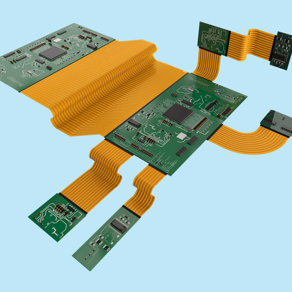
Flex rigid PCBs feature both flexible layers and rigid layers bonded into a single circuit board with components populated across both sections.
Here is a breakdown of how flex rigid PCBs are constructed:
- Rigid substrate cores – Forms the backbone and main structure
- Flexible dielectric films – Bonded to the rigid cores to allow dynamic flexing
- Adhesive layers – Bond the flexible and rigid materials together
- Copper foil layers – Standard PCB conductor layers
- Cover layers – Protective coatings such as solder mask and silkscreen
Rigid Cores
The rigid sections of the PCB will contain fiberglass-reinforced rigid laminate cores such as common FR-4 material. These provide mechanical strength for the PCB.
Flexible Films
The flexible sections are composed of thin polyimide films. These are extremely thin plastic sheets that allow for repeated contortion and bending. KaptonTM film and flex-grade epoxies are commonly used.
Bonding Adhesive
To combine the separate rigid and flex materials into a single PCB, adhesive layers are used in between. These are specially formulated “bonding films” designed to join the disparate materials together.
Copper Foil
Like any PCB, thin copper foils are laminated onto the substrate layers to form the electrical traces and pads. Trace impedance needs special consideration between the different materials.
Protective Coatings
The outer surfaces will be coated with solder mask to prevent shorting and silkscreen for markings. Special flex solder masks allow bending without cracking.
Cross Section Diagram
This cross section diagram visually depicts the layered construction:
+--------------------------------------------+
|        Soldermask         |        |       |
+--------------------------------------------+
|                    Copper Foil Layers         |
+--------------------------------------------+
|  Bonding Adhesive/Flexible Dielectric Films |
+--------------------------------------------+
         Rigid FR4 Substrate Cores
+--------------------------------------------+
First, the rigid cores provide mechanical support. Flexible films are attached on one or both sides using bonding adhesive. Copper traces are built up, then protective soldermask applied as the final coating.
The rigid sections maintain normal PCB thickness while the flex areas are extremely thin for flexibility. Interconnects and vias transition between sections.
Flex Rigid PCB Design Considerations
Designing a flex rigid PCB requires special considerations for the combination of materials and applications across both rigid and flex sections of the board:
Flex/Rigid Transition: The intersections between rigid and flex require gradual angles to avoid sharp bends that will wear quickly. Avoiding 90° intersections is advised whenever possible.
Trace Layout: Must account for dynamic bending on flex sections that will cause trace movement and expansion/contraction. Maintaining consistent trace geometries is advised.
Component Placement: Heavier, larger components should be placed on rigid sections while lighter components can be placed on flexible areas.
Vias/Interconnects: The transitions between layers may require stepped vias or specialized interconnects when crossing between rigid and flex sections.
Thermal Management: The flex area has less thermal mass. Power planes and copper fills may help dissipate heat, and care must be taken with heat generating components.
Stiffening Elements: Strategically placed components, copper fills, or even bonding stiffeners can help strengthen high-stress areas and prevent flex cracks.
Following established design rules for flex-to-rigid transitions and minimizing unnecessary flexing cycles will produce reliable, long lifetime PCBs.
Types of Flex Rigid PCBs
There are a few common configurations of flex rigid PCBs designed for specific mechanical packaging and electrical interconnection requirements:
Multilayer Rigid-Flex – Multiple rigid boards interconnected via flexible circuits in between, allowing a 3D stackup.
Rigid-Flex-Rigid – Traditional flex circuit with stiffened areas on one or both ends. Dynamic flex section in middle.
Curved Rigid-Flex – Rigid boards joined by arched, curved flex circuit to contour surfaces or mechanisms.
Folding Rigid-Flex – Accordion-style flex circuits with rigid sections that allow compact folding into tight spaces.
Typical Applications of Flex Rigid PCBs
Because of their unique properties combining compact flexibility and rigid stability, flex rigid PCBs are designed into many products where complex electrical connections meet dynamic mechanical demands:
Wearable electronics – Conform to curved surfaces and human movement
Medical devices – Embedded monitoring with flexible cabling
Robotics joints – Interconnections that can twist/bend with motion
Defense systems – Rugged electronics that can withstand vibration/shock
Consumer gadgets – Folding/sliding mechanics and small form factors
Automotive assemblies – Dynamic vehicle subsystems
Their adaptability allows flex rigid PCBs to provide interconnectivity across almost any application where both flexibility and strength are required in the circuit board itself.
Flex Rigid PCB Material Selection
Choosing the proper base materials is critical to designing a flex rigid PCB fit for each specific application across the rigid and flex sections of the board:
Rigid material
- FR-4 – Most common rigid PCB material
- High-Tg alternatives – For higher temperature or demanding environments
- Metal core substrates – For maximum thermal performance
Flex material
- Polyimide films – KaptonTM or equivalent alternates
- Adhesive – Bonding film designed for rigid-flex bonding
- Coverlay – Soldermask rated for dynamic flexing
Environmental requirements, electrical demands, mechanical spectrum, and thermal loads all factor into the proper selection of base materials needed for manufacturing quality flex rigid PCBs.
Quality Control and Testing
Verifying assembly quality and reliable system performance requires specialized testing focused on the requirements of rigid-flex designs:
Visual Inspection – Confirm proper rigid/flex intersections, trace geometries, pad alignments, and coating coverage.
Net List Testing – Continuity testing ensures correct interconnectivity between layers and sections.
Flex Cycle Testing – Simulates required dynamic bending cycles to validate robustness.
Vibration Testing – Confirms durability under mechanical vibration expected within application.
Thermal Stress Testing – Extreme heat/cold cycles combined with harsh temperature ramps.
Coating Adhesion Testing – Validate coating strength by applying peel or shear force.
With rigorous inspection testing combined with technological sophistication, flex rigid PCBs can deliver reliable electronic interconnectivity within mechanically demanding applications.
Flex Rigid PCB vs Rigid Flex PCB

While often used interchangeably, “flex rigid PCB” and “rigid flex PCB” can have distinct meanings:
Flex Rigid PCB
- Emphasizes the flexible nature of the circuit board
- Focused on dynamic mechanical features
- Flexible substrate with localized rigid sections only where needed
Rigid Flex PCB
- Emphasizes the rigid PCB foundation
- Focused on stability and rigidity for electronics
- Rigid substrate with only minimum localized flex areas
The naming distinction highlights the primary intention driving the design priorities of the PCB layout.
Flex rigid focuses first on contouring and mechanical dynamism enabled by large flexible sections. Rigidity is only secondarily required in selected areas.
Rigid flex focuses first on stability, temperature resistance, and strength provided by expansive rigid sections. Flexibility is only secondarily required in select small areas.
In practice, the terms are often used interchangeably. But this delineation can provide insight into the exact priority balancing of capabilities within a given hybrid rigid flex circuit board design.
Benefits and Advantages
Flex rigid PCBs provide a number of important benefits and advantages over traditional rigid PCBs:
Lightweight
Thin flexible substrates weigh less than thick rigid boards. This enables lighter weight finished electronics.
Increased Reliability
Dynamic flexing uniformly distributes stress over curves instead of focused bending pressure points.
Enhanced Mechanics
Moving mechanisms can be embedded within flexing section of singular circuit board.
Space Savings
Allows compact, thinner finished assemblies by consolidating interconnects.
Design Freedom
New applications are possible with unhindered contours and unique layouts.
Simplified Assembly
Combining multiple rigid boards’ connections into a single flex assembly.
These traits enable innovative electronic product designs combining digital circuits into new dynamic mechanical forms previously unachievable.
Careful flex rigid PCB design can successfully withstand mechanical rigors superior to strict rigid-only circuit boards. Their specialized construction comes with higher costs, but the benefits outweigh expense for suitable applications.
Flex Rigid PCB Design Guidelines
To produce a successful flex rigid PCB, designers must follow a specific set of design guidelines addressing the hybrid material properties.
Trace Routing
- Use teardrop pads on flex-section traces to strengthen solder joints against dynamic bending forces
- Avoid 90° trace angles to prevent stress concentration points due to repeated flexing
- Minimize unsupported trace lengths to reduce fracturing under bending loads
Transitions Between Sections
- Utilize minimum clearance trace routing and pad placement shifts when crossing between sections
- Eliminate rigid-to-flex air gaps with flexible solder mask or cover film
- Design smoother angles rather than sharp 90° bends at intersections
Component Placement
- Position larger, heavier components on rigid sections for stability
- Ensure clearance for dynamic components near edges of any rigid sections
- Consider focused stiffening elements under tall, heavy components
Copper and Grounds
- Use copper fills and planes for thermal conduction and electromagnetic shielding where needed
- Allow sufficient isolation spacing between copper pours with high voltage differences
Specialized Interconnections
- Employ stepped vias, staggered pads, or flex tongues when transitioning layers between sections
- Verify full pad contact through pragmatically contorted range of flexing motion
Following established guidelines helps optimize flex rigid PCB layouts for manufacturing and functional reliability.
Conclusion
With both rigid stability and flexible dynamism combined into singular circuit boards, flex rigid PCBs bridge connectivity challenges across compact modern electronic devices. They integrate digital electronics into the contours mechanisms once unachievable
FQA about Flex Rigid PCBs
What are some typical specifications for flex rigid PCBs?
Typical specifications include:
- Rigid section thickness: 1.2-1.6mm
- Flex section thickness: 25-100μm
- Flexible substrate materials: Polyimide, PET, PEN films
- Rigid substrate materials: FR4, BT, PPO
- Layer counts: 4-12 layers
- Line width/space: Minimum 8/8mil lines
- Bend radius: As low as 2-5X dielectric thickness
What types of files are used in flex rigid PCB design?
Common file types include:
- Gerber files – Standard PCB fabrication data
- 3D step models – Allow evaluation for fit, clearance, etc
- IPC-D-310 drawings – Design documentation details
- Master fabrication drawing – Fully defines scope of work
Should components be mounted on both rigid and flex areas?
Lightweight components like resistors and chips can be mounted directly on flexible sections, but any taller, heavier, or high-pin-count components should be mounted on rigid sections for maximum stability under shock/vibration.
How are vias constructed on flex rigid PCBs?
Plated through hole vias with annular rings are used in rigid sections while stacked vias or flexible interconnect “vias” made with multiple pads are used in the flex area. Blind and buried vias connect internal layers.
What are important considerations for component placement?
Components should be positioned to minimize required flexing by the traces so bending forces don’t overstress solder joints. Clearances must allow for maximum dynamic component movement extremes across the range of flexing motion.