

What is a PCB transformer?
Introduction to PCB Transformers
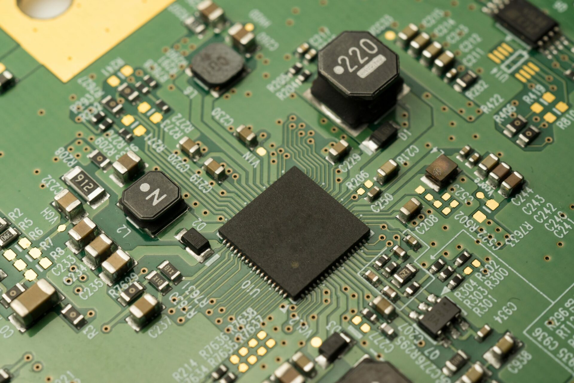
A printed circuit board (PCB) transformer is a type of transformer designed to be installed directly on a printed circuit board (PCB) in an electronic device. PCB transformers provide stepped up or stepped down voltage levels required for various semiconductor components and circuits on a PCB.
PCB transformers offer several advantages over traditional wire-wound transformers:
Smaller Size
PCB transformers are much more compact than wire-wound versions, allowing for smaller overall device sizes. Eliminating the need for external transformers saves significant space.
Lower Cost
PCB transformers leverage the existing PCB manufacturing process, eliminating the need for a separate transformer manufacturing and installation process. This results in lower per-unit costs at production scale.
Higher Reliability
With no connecting wires, soldered joints or wiring harnesses required, PCB transformers avoid reliability issues caused by faulty connections and failed components common in larger wire-wound transformers. The bonding of traces directly to the PCB substrate improves mechanical rigidity and longevity.
Design Flexibility
PCB transformers can be designed with precise electrical characteristics tailored to the exact needs of the circuit design. Voltage, current, frequency response and other parameters can be dialed in during the PCB layout process.
How PCB Transformers Work
PCB transformers work on the same principles of electromagnetic induction as traditional wire-wound transformers, just implemented directly on a printed circuit board substrate:
The transformer consists of two inductive coils:
- Primary coil – The input coil that energy is supplied to
- Secondary coil – The output coil at the transformed voltage level
The coils are formed by conductive traces usually made of copper, built up through the same lithographic PCB fabrication process as the rest of the board.
The coils are arranged close together to allow magnetic flux linkage between them, but with sufficient spacing to prevent shorts and direct current conduction. By altering the ratio of turns between the coils, voltage levels can be increased (stepped up) or decreased (stepped down) from input to output according to the turns ratio.
When an alternating excitation voltage is applied to the primary coil, the changing current creates an alternating magnetic field in the core which induces a voltage in the secondary coil through electromagnetic induction. This induced voltage then drives the load.
PCB Transformer Types
There are a few common varieties of printed circuit board transformers:
Planar Transformers
Planar transformers use a flat coil structure with two overlapping windings fabricated directly on the PCB surface. This provides vertical integration and keeps vertical space requirements to a minimum.
Spiral Transformers
Spiral transformers use square or hexagonal coil geometries wound inward like a spiral, allowing for high coupling efficiency and high self-resonant frequencies. The spiral pattern minimizes stray capacitance between windings.
Toroidal Transformers
Toroidal PCB transformers wrap coils around ring-shaped ferrite cores to confine magnetic flux and reduce external field radiation for high efficiency. The circular symmetry promotes excellent coupling between primary and secondary windings.
Comparison of Different PCB Transformer Types
| Parameter | Planar | Spiral | Toroidal |
|-|-|-|-|
|Size | Compact vertical profile | Larger surface area | Mid-range |
|Self-capacitance| Moderate | Low | High |
|Efficiency| Moderate | High | Highest |
|Complexity| Simple | Moderate | Challenging |
|Cost | Low | Mid-range | Highest |
PCB Transformer Materials
PCB transformers are constructed using conductive windings and magnetic core materials built up through the board fabrication process:
Conductive Windings
The conductive coils are typically made from copper or aluminum traces, just like regular PCB tracks. The thickness and width of these traces determines their current handling capability. Common thicknesses range from 35μm up to 400μm.
Magnetic Cores
The core serves to confine and channel magnetic flux to optimize coupling between input and output windings. Core materials exhibit high permeability to facilitate magnetic conduction with minimal losses.
Common PCB transformer core materials include:
- Ferrite
- Iron alloys
- Amorphous metal alloys
- Ferromagnetic nanocrystalline material
These high permeability materials are usually implemented as part of the board substrate itself or applied via a separate fabrication process.
In coreless PCB transformer designs, no distinct core is used. An air or resin core relies instead on the natural magnetic properties of the PCB windings and base material. This simplifies manufacturing complexity slightly but reduces achievable coupling and efficiency.
PCB Transformer Production
PCB transformers are manufactured using many of the same processes used to produce standard printed circuit boards:
Printed Circuit Board Transformer Fabrication
- Design – The transformer is designed and simulations performed to define required trace dimensions and core characteristics
- Lamination – The base PCB substrate is combined with transformer core materials
- Conductive Layer – A layer of copper is laminated onto the substrate
- Photoresist – The coil pattern is transferred onto the copper layer using photolithographic processes
- Etching – Ferric chloride solution dissolves away unwanted copper areas
- Stripping – The remaining photoresist layer is removed
- Repeat – Further copper layers are added to produce multi-layer transformer windings
- Drilling – Holes are drilled for through-hole pin connections
- Testing – The electrical parameters are verified through testing
This approach maximizes compatibility with automated high-volume PCB fabrication processes and quality control checks.
Some additional steps are often incorporated for more complex transformer constructions:
- Multiple conductive layers to produce complex windings
- Additional core layers or materials
- Windings wrapped around ferrite cores
- HDI laser drilled microvias to produce intricate transformer structures with densely packed windings
Application of PCB Transformers
The applications of printed circuit board transformers span a wide variety of electronic devices:
Applications of PCB Transformers
- DC-DC converters
- Low voltage lighting (12V to 0.5V)
- Voltage regulation for microprocessors
- USB and USB Power Delivery implementations
- Laptop and mobile device chargers
- Gate driver boards
- On-board battery charging
- Power supplies
- Class D audio amplifiers
- Sensor excitation and measurement
Integrating the transformer directly into the printed circuit board allows reducing bulky wire-wound external transformers. This paves the way toward increasingly miniaturized device constructions.
The tailored response of PCB transformers also helps maximize power transfer efficiency in the end application across different voltage and current levels.
Benefits of Using PCB Transformers
PCB transformers offer numerous advantages over conventional discrete transformers:
Benefits of PCB Transformers
- Extremely compact footprint
- Lower overall cost
- Improved reliability from fewer faulty connections
- Facilitates automated mass production
- Compatible with SMD production processes
- Simplifies high density PCB integration
- Enables miniaturization of end products
- Easily integrated with control circuitry
- Excellent thermal performance through board spreading
- Optimized electrical parameters
- Elimination of parasitics associated with wires
- Design flexibility with choice of trace layouts
- High isolation voltage capabilities
With continuing improvements in PCB technology and fabrication techniques enabling better resolution, higher aspect ratios and denser component packing, PCB transformers will continue growing in popularity wherever space savings, safety improvements or cost reductions are needed.

Their seamless integration with the electronic circuits they support cements their role as a key technology in the future of small, efficient and reliable power conversion.
Limitations of PCB Transformers
While printed circuit board transformers provide valuable advantages, they also come with certain limitations:
Drawbacks of PCB Transformers
- Limited power handling capability relative to wire-wound transformers
- More difficult to build heavy gauge windings
- Winding patterns restricted by PCB design rules and process tolerances
- Lower achievable inductance compared to iron core varieties
- Core materials increase material cost and fabrication complexity
- Testing individual transformers requires specialized fixturing techniques
- Can suffer reduced reliability under high G-forces due to uneven PCB flexure
The continuing development path for PCB transformer technology revolves around pushing the boundaries in these areas through incremental fabrication process improvements and novel packaging arrangements.
Future Outlook
Several trends point toward greatly expanded use of printed circuit board transformers spanning into higher power applications:
Future PCB Transformer Development Trends
- Fabrication techniques facilitating thicker and higher resolution conductors
- Improved magnetic materials tailored to PCB integration
- Adoption of new winding arrangements to boost density and coupling efficiency
- Multi-axis laminations to cancel induced currents and minimize losses
- Novel construction approaches allowing extremely high isolation voltages
- Integration of control and support circuitry into transformer layers
- Onboard monitoring and analytics for safety
As performance characteristics continue improving, PCB transformers will transform power conversion circuit implementations across virtually all electronic industry verticals by unlocking unprecedented levels of miniaturization, efficiency, reliability, and cost economies.
This transition promises more capable yet cheaper-to-manufacture designs across all scales from milliwatt sensor modules to high current inverters and fast chargers. Their emergence stands poised to accelerate innovation across cutting-edge tech sectors.
Frequently Asked Questions
What is the main advantage of PCB transformers?
The main benefits of PCB transformers are dramatic space savings and lower costs that stem from integrating the transformer directly into the PCB assembly process instead of requiring an external discrete wired component.
What are the different types of PCB transformers?
Common types of PCB transformers include planar transformers with stacked windings, spiral transformers arranged as square or hexagonal coils, and toroidal transformers with doughnut/ring-shaped cores.
How much power can PCB transformers handle?
Typical PCB transformers support power handling of 1-10 watts for low power applications and up to approximately 200 watts for high power density versions. For heavier power loads, specialized assembly processes facilitate stacked PCB arrangements.
What determines the voltage transformation ratio?
The turns ratio between the number of conductive winding loops in the input and output transformer coils largely determines the voltage step up/down ratio that will result between the primary and secondary sides.
Can PCB transformers replace regular wire-wound transformers?
With continual improvements in achievable current, power handling and efficiency, PCB transformers will displace wire-wound versions across a growing range of applications to take advantage of their smaller size, lower cost and heightened reliability.