


What is PCB Layout?
PCB layout, also known as printed circuit board layout, is the process of designing the physical layout of a printed circuit board (PCB). It involves arranging the components, traces, and other features on the board to ensure proper functionality, manufacturability, and reliability of the electronic device.
The PCB layout process starts with a schematic diagram, which represents the electrical connections between components. The layout designer then translates this schematic into a physical layout, considering factors such as component placement, trace routing, power distribution, signal integrity, and manufacturing constraints.
Key Aspects of PCB Layout
- Component Placement: The placement of components on the PCB is crucial for several reasons:
- Minimizing the distance between connected components to reduce signal delays and improve signal integrity.
- Ensuring proper thermal management by placing heat-generating components in areas with adequate cooling.
- Optimizing the board space and making the design compact.
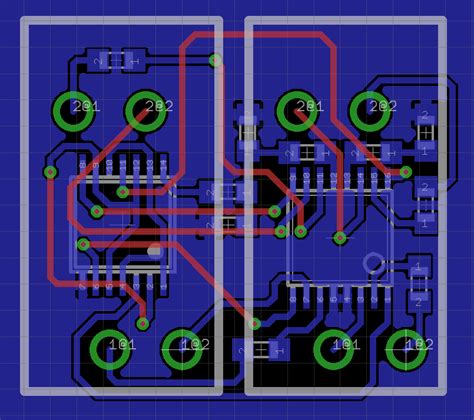
- Trace Routing: Traces are the copper paths that connect components on the PCB. Proper trace routing is essential for maintaining signal integrity and avoiding issues like crosstalk, electromagnetic interference (EMI), and signal reflections. The layout designer must consider factors such as trace width, spacing, and length when routing traces.
- Power Distribution: The PCB layout must ensure proper power distribution to all components. This involves designing power planes, ground planes, and power traces with adequate thickness to handle the required current. Proper power distribution helps minimize voltage drops, reduce noise, and improve overall system stability.
- Signal Integrity: Maintaining signal integrity is crucial in high-speed and sensitive designs. The layout designer must consider factors such as impedance matching, termination, and shielding to minimize signal distortion, reflections, and crosstalk. Techniques like differential pair routing and ground plane stitching are often used to improve signal integrity.
- Manufacturing Constraints: The PCB layout must adhere to manufacturing constraints to ensure the board can be reliably and cost-effectively produced. This includes considering factors such as minimum trace width and spacing, hole sizes, soldermask and silkscreen requirements, and panelization for mass production.
PCB Layout Design Process
The PCB layout design process typically involves the following steps:
- Schematic Review: The layout designer reviews the schematic diagram to understand the circuit functionality, component requirements, and connectivity.
- Component Placement: The designer places the components on the board, considering factors like signal flow, thermal management, and mechanical constraints.
- Power Distribution: Power planes, ground planes, and power traces are designed to provide stable and efficient power distribution to all components.
- Trace Routing: The designer routes the traces between components, following the schematic and considering signal integrity, EMI, and manufacturability.
- Design Rule Check (DRC): The layout undergoes a DRC to ensure it adheres to the specified design rules, such as minimum trace width, spacing, and hole sizes.
- Manufacturing Output: The final layout is generated in the form of Gerber files, drill files, and other manufacturing outputs required for PCB fabrication.

PCB Layout Software
There are several software tools available for PCB layout design. Some popular options include:
| Software | Company | Key Features |
|---|---|---|
| Altium Designer | Altium | Comprehensive PCB design suite, 3D modeling, simulation |
| EAGLE | Autodesk | Schematic capture, PCB layout, extensive component libraries |
| KiCad | Open Source | Free and open-source, schematic capture, PCB layout, 3D viewing |
| OrCAD PCB Designer | Cadence | Advanced PCB layout, constraint management, signal integrity analysis |
| PADS | Mentor Graphics | PCB layout, high-speed design, advanced routing capabilities |
These software tools provide a range of features and capabilities to streamline the PCB layout design process, from schematic capture to final manufacturing output generation.

Benefits of Professional PCB Layout Services
While it is possible to design PCB layouts in-house, many companies and individuals choose to outsource the task to professional PCB layout services. Here are some benefits of using professional PCB layout services:
- Expertise: Professional PCB layout designers have the knowledge and experience to tackle complex designs and ensure optimal performance, reliability, and manufacturability.
- Time Savings: Outsourcing PCB layout design allows companies to focus on their core competencies while leaving the layout work to experts, saving time and resources.
- Cost Efficiency: Professional PCB layout services often have access to advanced tools and technologies that may be cost-prohibitive for individual companies. Outsourcing can be more cost-effective than investing in expensive software and training.
- Quality Assurance: Professional PCB layout services follow industry standards and best practices to ensure high-quality designs that meet the required specifications and regulations.
- Scalability: PCB layout services can handle projects of various sizes and complexities, from simple single-layer boards to complex multi-layer designs with high-speed signals and dense component placement.

Choosing a PCB Layout Design Service
When selecting a PCB layout design service, consider the following factors:
- Experience: Look for a service provider with a proven track record in designing PCBs for applications similar to yours. Check their portfolio and customer testimonials to assess their expertise.
- Capabilities: Ensure the service provider has the necessary tools, software, and technology to handle your specific design requirements, such as high-speed design, RF design, or flex PCBs.
- Communication: Clear and effective communication is crucial for a successful PCB layout project. Choose a service provider that is responsive, communicates well, and keeps you informed throughout the design process.
- Turnaround Time: Consider the service provider’s typical turnaround times and their ability to meet your project deadlines. Some providers offer expedited services for time-critical projects.
- Cost: Obtain quotes from multiple service providers and compare their pricing. However, keep in mind that the lowest price may not always be the best option, as quality and expertise should also be considered.
Conclusion
PCB layout design is a critical step in the development of electronic devices. It involves arranging components, traces, and other features on the board to ensure proper functionality, manufacturability, and reliability. The PCB layout process considers factors such as component placement, trace routing, power distribution, signal integrity, and manufacturing constraints.
Outsourcing PCB layout design to professional services can offer benefits such as expertise, time savings, cost efficiency, quality assurance, and scalability. When choosing a PCB layout design service, consider factors like experience, capabilities, communication, turnaround time, and cost.
By leveraging the expertise of professional PCB layout services, companies can ensure their electronic devices are designed to the highest standards, optimized for performance, and ready for manufacturing.
Frequently Asked Questions (FAQ)
- What is the difference between PCB layout and PCB design?
PCB layout focuses on the physical arrangement of components, traces, and features on the board, while PCB design encompasses the entire process from schematic design to final manufacturing output, including PCB layout. - What are the common challenges in PCB layout design?
Common challenges include ensuring signal integrity, minimizing electromagnetic interference (EMI), optimizing component placement for thermal management, and adhering to manufacturing constraints. - How long does it take to complete a PCB layout design?
The time required for PCB layout design varies depending on the complexity of the design, the number of layers, and the experience of the designer. Simple designs can be completed in a few days, while complex designs may take several weeks. - What information is needed to start a PCB layout design?
To start a PCB layout design, you typically need a schematic diagram, a bill of materials (BOM), component footprints and datasheets, design requirements and constraints, and any specific manufacturing guidelines. - Can PCB layout design services handle both prototype and production quantities?
Yes, most PCB layout design services can handle both prototype and production quantities. They can design the layout for initial prototyping and then optimize it for mass production, considering factors like panelization and manufacturing yield.