How long does PCB fabrication take?
Introduction to PCB fabrication process
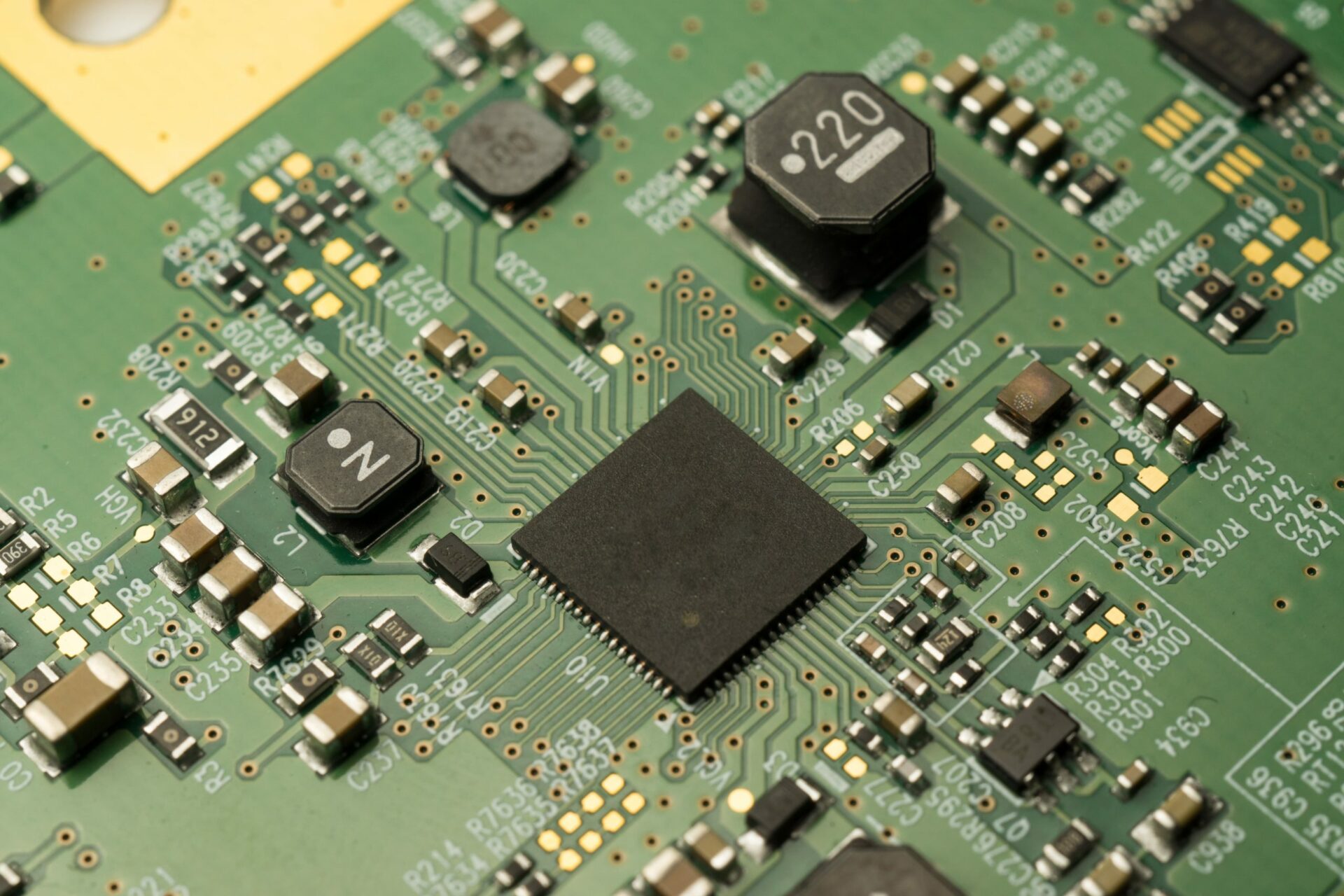
Printed circuit boards (PCBs) form the backbone of electronic devices and products. They provide the interconnects between various components and integrated circuits in an electronic system. The PCB fabrication process transforms the PCB design files into actual physical boards ready for component assembly. It involves several steps including:
- CAM (Computer Aided Manufacturing)
- Panelization
- Imaging
- Etching
- Stripping
- Testing and inspection
- Solder mask application
- Silkscreen printing
- Routing/scoring
- Final testing and inspection

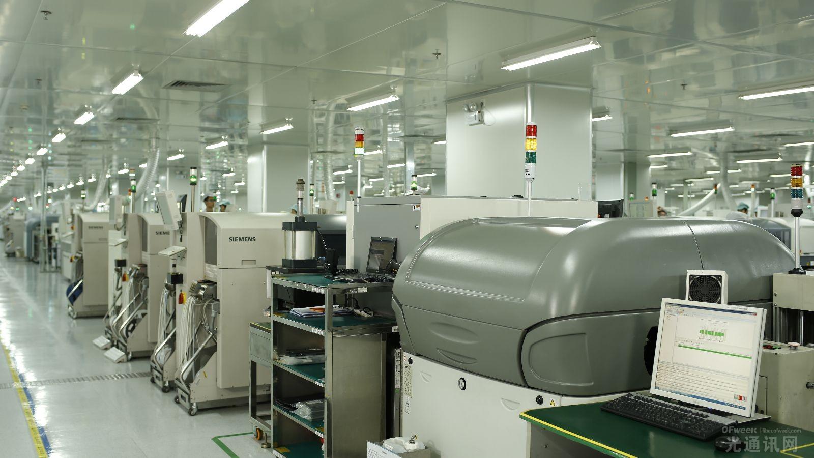
The time required to fabricate a PCB batch depends on various factors like board complexity, number of layers, order quantity, fabrication techniques used, and the PCB manufacturer’s production capacity and lead times.
What determines PCB fabrication lead time?
- Board complexity – More complex boards with high component density, fine features, and tight tolerances take longer to manufacture. They require more careful processing and testing.
- Number of layers – Multilayer boards take longer than simple 2-4 layer boards due to additional lamination and drilling time.
- Order quantity – Batch size impacts queue times. Smaller quantities normally have shorter lead times.
- Fabrication technique – Technique used whether standard, advanced, or high-density interconnect (HDI) affects process time.
- Manufacturer capacity – Large, automated factories with high output have shorter lead times. Boutiques tend to take longer.
- Location – Domestic manufacturers tend to have quicker turnaround over overseas.
- Computer aids – Modern CAM, imaging, and testing tools speed up fabrication.
PCB fabrication process steps and time estimates
Here is a typical sequence of PCB fabrication steps with estimates of time taken:
CAM and panelization
- PCB design data preparation – 1-3 days
- Panelization and arrangement – Few hours to 1 day
Once the design files are received, the manufacturer runs design rule checks, optimizes files for production, and arranges boards based on panel sizes. Panelization involves grouping multiple PCB designs into larger panels to maximize manufacturing efficiency.
Simple designs may just take 1-3 days for CAM processing whereas complex designs with many dense boards may take 3-5 days.
Imaging
- Photolithography – 1-3 days
- Etching – 2-6 hours
- Stripping – 1-2 hours
The panels go through an imaging process where the desired copper pattern is printed onto the boards. This involves applying a photosensitive coating, exposing the coating to UV through a mask, developing the images, and then etching away copper from undesired areas.
Photolithography and etching may take 1-5 days depending on complexity. Stripping off the remaining photoresist takes 1-3 hours.
Layer lamination
- Layer pressing – 2-8 hours per lamination cycle
- Drilling – 1-5 hours
- Deburring – 1-2 hours
For multilayer boards, individual cores are laminated using bonding sheets. Alignment, heating, cooling, and pressure cycles take several hours per layer. The layers then undergo precision drilling to create vertical interconnects between layers. Deburring removes remnants from drilling.
Complex boards may need special preparation between laminations. The time for this stage ranges from 1 day for simple 4-6 layer boards, up to 2 weeks for high layer count boards.
Final finishes
- Soldermask coating – 1-2 days
- Silkscreen printing – 4-8 hours
- Surface finishing – 1 day
- Routing and scoring – 2-5 hours
- Final testing – 1-3 days
The nearly finished boards now undergo solder masking to prevent solder bridges, silkscreen printing for markings, chemical processes for surface finishes, and precision scoring/routing to facilitate assembly. They then undergo final testing like bare-board electrical testing, automated optical inspection (AOI), X-Ray inspection etc. before shipping.
This stage normally takes 3-5 days but could be 1-2 weeks for very complex boards requiring extensive testing.
Summary of fabrication stages and time estimates
Here is a summary table with typical time estimates for key PCB fabrication steps:
| Fabrication Stage | Description | Time Estimate |
|---|---|---|
| CAM and Panelization | Data prep and panelizing | 1 – 5 days |
| Imaging | Photolithography, etching, stripping | 1 – 5 days |
| Layer Lamination* | Layer alignment and pressing | 1 – 14 days |
| Drilling* | Through-hole drilling and deburring | 1 – 2 days |
| Final Finishes | Soldermask, silkscreen, surface finish | 1 – 2 days |
| Testing | Electrical, AOI, X-Ray testing | 1 – 3 days |
| Total Time | 5 days – 4 weeks |
As seen above, fabrication times vary widely from a few days for simple double-sided boards to 4 weeks for complex multilayer boards requiring advanced processing. Factors like order quantity, manufacturer schedules, shipping, and others also affect overall time from order to delivery.
How to reduce PCB fabrication time?
Here are some tips to help reduce overall fabrication time for your PCBs:
- Optimize design rules and constraints – Use wide tolerances wherever possible, avoid unnecessarily fine features.
- Modularize complex designs – Break large boards into smaller sub-assemblies to simplify manufacturing
- Reduce unnecessary testpoints – Minimize testpoints unless essential for quality validation.
- Choose panel-friendly dimensions – Design board sizes to maximize panel utilization ratios.
- Consolidate orders – Club together multiple designs rather than small fragmented orders.
- Discuss time constraints – Clearly communicate your schedule needs to your PCB partner early.
- Choose quick-turn domestic shops – Local manufacturers have shorter pipelines than overseas.
- Pay for expedited processing – Many fabricators offer faster processing for urgent orders.
While the above tips help reduce lead time, you also need to account for reasonable processing variability across different board complexities. Planning your projects accordingly and adding buffers help prevent delays down the line.
FQA
What is the fastest PCB fabrication time?
The fastest fabrication times are 1-3 days from order to delivery. This is typically only possible on very simple 2-4 layer boards made singly or in small batches (under 10 units) using quick-turn domestic PCB shops. Typical parameters for 3 day delivery:
- 2-4 layers
- Standard FR4 material
- Under 4 sq. inches size
- Minimum track/space width 6 mil
- 1.5 oz copper thickness
- Through hole pads only
- No impedance control needed
- very simple testing
For such boards, it’s possible to complete all fabrication steps within 1-3 days by running small batches through the manufacturing line ahead of other orders.
What is the normal PCB fabrication lead time?
For medium complexity boards made in small-medium quantities (10-100 units), the typical lead times range from 5 days to 2 weeks. This covers standard 4-8 layer boards with SMT pads, basic impedance control, and common soldermask/silkscreen requirements.
Boards requiring advanced processing like HDI, flex/rigid-flex construction, exotic materials, or complex testing usually need 3-6 weeks. High density boards like server motherboards fall in the 6-8 weeks category owing to extensive fabrication and verification procedures involved.
Which step consumes the most time in PCB fabrication?
For multilayer boards, the layer lamination processes often take up the most time ranging from days to even weeks for very high layer counts (>16). Steps like alignment, press bonding, surface preparation between cycles, and post-lamination recovery are very time intensive and run for hours per layer. These cannot be easily accelerated by throwing more equipment or labor at it.

For simpler double-sided or flex boards, etching and imaging may take the longest depending on artwork complexity. Shops balance the line capacity between etchant tanks, exposure equipment, washing stations to prevent bottlenecks. Delays can crop up if one particular process exceeds capacity.
Can I pay extra for faster fabrication?
Most PCB manufacturers offer expedited services for urgent orders by prioritizing them ahead of other boards in their production schedule. This could get your boards fabricated in just 1-2 days. However, qualifications apply based on order size, board complexity, and manufacturer capability.
The premium percentage charged for expedited fabrication varies based on manufacturer and demand conditions, but typically ranges from 25% to 100% over standard pricing. Beyond a threshold level, increasing throughput causes diminishing returns due to equipment/labor constraints at fabrication facilities.
What is a reasonable fabrication lead time to expect?
A reasonable expectation would be:
- 1-3 days for simple double-sided boards (for prototyping)
- 5-7 days for moderate complexity multilayer boards (for pre-production)
- 3-4 weeks for intricate HDI based designs (for production)
It’s prudent to allocate 2X buffers over typical times when planning your projects and account for potential manufacturing delays or iteration cycles required before design sign-off. Keep an open channel of communication with your PCB partner and plan early during product development to prevent delays in end deployment.


