

Introduction to Polygon Pour and Rigid Flex PCBs
Polygon pour is a essential technique used in PCB design to create solid copper areas for power distribution, shielding, and ground planes. It involves filling a defined area with a solid copper pour, which is connected to a specific net or signal. Polygon pour helps to improve signal integrity, reduce electromagnetic interference (EMI), and dissipate heat more effectively.
Rigid flex PCBs are a combination of rigid and Flexible PCBs, allowing for a more compact and versatile design. These boards consist of rigid sections connected by flexible sections, enabling the PCB to be folded or bent to fit into tight spaces or conform to unique shapes. Rigid flex PCBs are commonly used in applications that require high reliability, such as aerospace, military, and medical devices.
Benefits of Polygon Pour in PCB Design
- Improved power distribution
- Enhanced signal integrity
- Reduced electromagnetic interference (EMI)
- Better heat dissipation
- Increased mechanical stability
Advantages of Rigid Flex PCBs
- Space savings and compact design
- Improved reliability and durability
- Reduced assembly time and costs
- Enhanced flexibility and conformity
- Elimination of connectors and cables
Altium Designer and Polygon Pour
Altium Designer is a powerful PCB design software that offers a comprehensive set of tools for creating high-quality PCBs. One of its key features is the ability to create and manage polygon pours efficiently. Altium Designer provides a user-friendly interface for defining polygon pour areas, setting their properties, and ensuring proper connectivity.
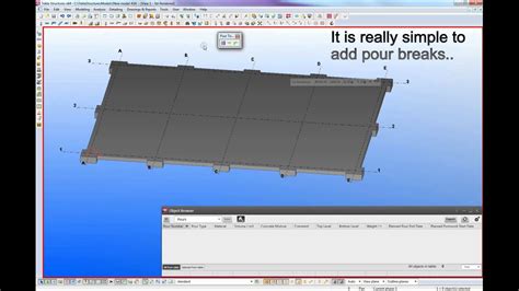
Creating Polygon Pours in Altium Designer
- Select the “Pour” command from the “Place” menu or toolbar
- Define the polygon pour area using the available drawing tools
- Set the polygon pour properties, such as the net, layer, and clearance settings
- Perform a design rule check (DRC) to ensure the polygon pour meets the specified rules
- Regenerate the polygon pour to update any changes
Managing Polygon Pours in Altium Designer
- Use the “Properties” panel to modify the polygon pour settings
- Employ the “Polygon Manager” to view and edit all polygon pours in the design
- Utilize the “Polygon Connectivity” tool to check and resolve connectivity issues
- Apply “Polygon Cutouts” to create voids or openings within the polygon pour
- Leverage “Polygon Pour Order” to control the priority of overlapping polygon pours

Rigid Flex Split Lines and Polygon Pour Breaks
When designing rigid flex PCBs, it’s essential to consider the placement of split lines, which define the boundaries between the rigid and flexible sections. These split lines can sometimes cause issues with polygon pours, leading to unintended breaks or disconnects in the copper areas.
Common Causes of Polygon Pour Breaks on Split Lines
- Incorrect split line placement or alignment
- Insufficient clearance between the split line and polygon pour
- Improper layer stackup or copper balance
- Inadequate bend radius or flex region design
- Manufacturing limitations or constraints
Strategies to Avoid Polygon Pour Breaks on Split Lines
- Ensure proper split line placement and alignment with the PCB Layout
- Maintain adequate clearance between the split line and polygon pour
- Optimize the layer stackup and copper balance for the rigid flex design
- Adhere to recommended bend radius and flex region guidelines
- Collaborate with the manufacturer to address any specific limitations or requirements

Best Practices for Polygon Pour in Rigid Flex PCBs
To minimize the risk of polygon pour breaks on split lines and ensure a robust rigid flex PCB design, consider the following best practices:
- Plan the split line locations carefully, considering the mechanical and electrical requirements
- Use a consistent and symmetrical layer stackup for the rigid and flex sections
- Maintain a uniform copper balance across the layers to minimize stress and warping
- Provide sufficient clearance between the polygon pour and split line, as per the manufacturer’s guidelines
- Utilize teardrops or anchoring features to reinforce the connections at the split line interfaces
Polygon Pour Clearance Guidelines for Rigid Flex PCBs
| Clearance Type | Minimum Distance |
|---|---|
| Split Line to Polygon Pour | 0.2 mm |
| Polygon Pour to Component Pad | 0.25 mm |
| Polygon Pour to Via | 0.2 mm |
| Polygon Pour to Board Edge | 0.5 mm |
Note: These values are general guidelines and may vary depending on the manufacturer and specific design requirements.
Layer Stackup Considerations for Rigid Flex PCBs
When designing the layer stackup for a rigid flex PCB, consider the following factors:
- Use a symmetrical stackup to minimize warping and stress
- Maintain a consistent dielectric thickness for the rigid and flex sections
- Choose appropriate materials for the flex layers, such as polyimide or LCP
- Incorporate shielding layers or ground planes to improve signal integrity and EMI performance
- Collaborate with the manufacturer to ensure the stackup meets their capabilities and requirements

Troubleshooting Polygon Pour Breaks on Rigid Flex Split Lines
Despite following best practices and guidelines, polygon pour breaks may still occur on rigid flex split lines. In such cases, troubleshooting the issue is crucial to identify the root cause and implement appropriate solutions.
Common Troubleshooting Steps
- Review the split line placement and alignment with the PCB layout
- Check the clearance settings between the polygon pour and split line
- Analyze the layer stackup and copper balance for any discrepancies
- Verify the bend radius and flex region design against the manufacturer’s guidelines
- Consult with the manufacturer to identify any specific limitations or requirements
Resolving Polygon Pour Breaks on Split Lines
Once the root cause of the polygon pour break is identified, implement the necessary corrective actions:
- Adjust the split line placement or alignment to ensure proper positioning
- Modify the clearance settings to provide adequate space between the polygon pour and split line
- Optimize the layer stackup and copper balance to minimize stress and warping
- Revise the bend radius or flex region design to comply with the manufacturer’s guidelines
- Collaborate with the manufacturer to address any specific issues or constraints
Conclusion
Polygon pour breaks on rigid flex split lines can be a challenging issue in PCB design, but with proper planning, best practices, and troubleshooting techniques, these issues can be effectively mitigated. By understanding the causes of polygon pour breaks, following design guidelines, and collaborating with the manufacturer, designers can ensure the integrity and reliability of their rigid flex PCBs.
Key Takeaways
- Polygon pour is a critical technique for power distribution, shielding, and ground planes in PCB design
- Rigid flex PCBs offer space savings, improved reliability, and enhanced flexibility
- Altium Designer provides powerful tools for creating and managing polygon pours efficiently
- Split line placement, clearance settings, layer stackup, and bend radius are crucial factors in avoiding polygon pour breaks
- Following best practices and troubleshooting techniques can help resolve polygon pour breaks on rigid flex split lines
Frequently Asked Questions (FAQ)
1. What is polygon pour, and why is it important in PCB design?
Polygon pour is a technique used in PCB design to create solid copper areas for power distribution, shielding, and ground planes. It helps to improve signal integrity, reduce EMI, and dissipate heat more effectively.
2. What are rigid flex PCBs, and what are their advantages?
Rigid flex PCBs are a combination of rigid and flexible PCBs, allowing for a more compact and versatile design. They offer space savings, improved reliability, reduced assembly time and costs, and enhanced flexibility.
3. How can I create and manage polygon pours in Altium Designer?
In Altium Designer, you can create polygon pours using the “Pour” command, define the pour area, and set the properties. You can manage polygon pours using the “Properties” panel, “Polygon Manager,” and other tools.
4. What causes polygon pour breaks on rigid flex split lines?
Polygon pour breaks on rigid flex split lines can be caused by incorrect split line placement, insufficient clearance, improper layer stackup or copper balance, inadequate bend radius, or manufacturing limitations.
5. How can I troubleshoot and resolve polygon pour breaks on split lines?
To troubleshoot polygon pour breaks, review the split line placement, check clearance settings, analyze the layer stackup and copper balance, verify the bend radius and flex region design, and consult with the manufacturer. Implement corrective actions based on the identified root cause.