

Introduction
Rigid-flex PCBs, also known as flex-rigid boards, combine rigid and flexible circuitry into a single assembly. They provide solutions for complex electronics packaging problems and enable 3D wiring optimization not possible with rigid PCBs alone. With 24 layers now possible, rigid-flex continues to enable further miniaturization and functionality. This article will provide an overview of 24 layer rigid-flex PCB technology, design considerations, manufacturing processes, and applications.
What is a 24 Layer Rigid Flex PCB?
A 24 layer rigid-flex PCB contains both rigid and flexible substrates laminated together into a single circuit assembly. The rigid sections provide mechanical support while the flexible sections enable dynamic flexing, folding and wrapping around structures. 24 layer stacks enable high density interconnections by utilizing the Z-axis for routing. This allows the integration of more components and circuitry into a compact 3D package.
In a 24 layer rigid-flex, at least one section contains a 24 layer PCB stackup. This may be in the rigid section or span both rigid and flex zones. The stackup will contain layers of laminated copper and dielectric. Popular dielectrics include FR-4, polyimide, PTFE composites, and others. The thin flexible sections allow dynamic flexing of the assembly. Polyimide films like Kapton® are commonly used. The rigid and flex sections are precisely aligned and laminated together into a single circuit board.
Benefits of 24 Layers
The key benefits of 24 layer rigid-flex PCBs include:
- Extremely high interconnect density and component packaging
- Integration of rigid and flex circuits into 3D assemblies
- Enable creative industrial design and ergonomics
- Folding and shaping into complex geometries
- Reduced weight and space requirements
- Eliminate connectors between separate PCBs
- Improved high speed performance
- Partition circuits across rigid and flex areas
- Reliability from laminated interconnects vs cables
Design Considerations
Designing a 24 layer rigid-flex PCB requires special considerations for layout, stackup, materials, transitions, etc. Here are some key guidelines:
Stackup – Proper layer stackup is critical for performance. Key factors are impedance control, noise reduction, signal integrity and power delivery. Stacking sequence, dielectric materials and copper weights should be optimized.
Routing – Careful routing practices must be followed. Trace widths, spacing, vias, planes, and impedance control take priority. Split power and ground planes help isolate noise.
Transitions – The transitions between rigid and flex require special attention. Mechanical stress must be minimized and impedance tuned. Special materials or flexible solder masks are used.
Flex Bending – Dynamic flexing requires management of stresses. Minimum bend radii and copper elongation should be considered. Strategic placement of components reduces strain.
Materials – Material selection impacts reliability. Consider thermal, mechanical, electrical and CTE properties. Mix materials to optimize regions.
DFM – Following good DFM rules is mandatory. Allow for tolerances, panel utilization, drilling access, etc. This ensures manufacturability.
Proper design tools, simulation, prototyping and manufacturer collaboration is key to optimizing 24 layer rigid-flex boards.
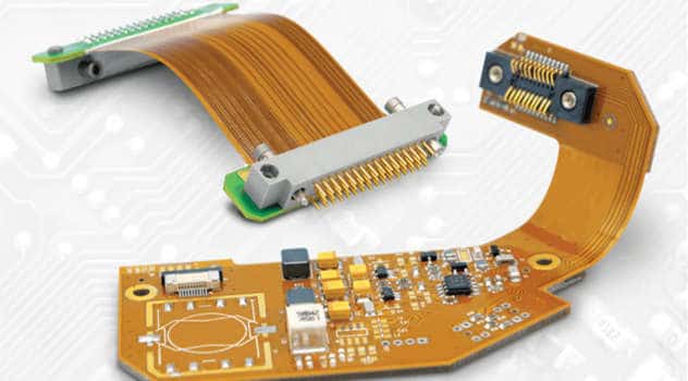
Application Example
Here is an example 6 layer rigid-flex PCB design highlighting some of the key layout considerations:
Simple 6 Layer Rigid Flex PCB Example (Image Credit: Altium)
- Rigid sections provide mechanical structure
- Flexible folds allow 3D packaging
- Careful component placement on flex areas
- Strategic layer stackup for performance
- Smooth impedance and reliability at transitions
- Kapton flexible material between layers
- Stress relief features on flex bends
24 Layer Rigid Flex Manufacturing
Producing 24 layer rigid-flex PCBs requires advanced manufacturing techniques and tight process controls. Here is an overview of the complex multilayer fabrication process:
Layer Preparation
- Photolithography forms circuit patterns on treated copper foils
- Etching removes unwanted copper, leaving traces
- Laminate bonding attaches circuit foils to dielectric cores
- Drilling provides through hole interconnections
- Plating deposits copper on hole walls
- Outer layers are processed similarly
Lamination
- Sheet layers are precisely aligned and stacked
- The layup is vacuum pressed at high heat and pressure
- Layers are fused into a single board with laminating resin
- Alignment is critical for layer-to-layer connections
Finishing
- Solder mask coats and insulates exposed traces
- Silkscreen provides component legends and markings
- Surface finishes protect pads and traces
- Edge connectors are added if required
- Vias and holes are plugged for soldering
- Test and inspection ensures quality
Assembly
- Components are accurately placed using solder paste
- Reflow soldering permanently attaches parts
- Additional testing validates operation
- Conformal coating protects against environment
Proper packaging, handling and quality procedures are followed throughout. The result is a high performance, reliable 24 layer rigid-flex PCB assembly ready for application.
Applications of 24 Layer Rigid Flex PCBs
The unique benefits of rigid-flex PCBs with high layer counts make them well suited for many advanced applications:
Aerospace and Defense
- Avionics systems with complex wiring
- Missile guidance systems
- UAVs with dimensional constraints
- Drones requiring flexing wings
Medical Electronics
- Implantable devices with compact wiring
- Hearing aids fitting the ear shape
- Endoscopes with flexible tubes
- Sensors conforming to the body
Consumer Electronics
- Foldable smartphones and tablets
- Wearable devices with dynamic flexing
- Digital cameras with pop-up features
Automotive Electronics
- Dashboard electronics conforming to shapes
- Engine control units in tight spaces
- ADAS and sensors requiring compactness
Internet of Things (IoT)
- Networked sensor nodes with small form factor
- Flexible circuits integrated into “smart” objects
- Conformal antennas and wireless modules
24 layer rigid-flex enables endless possibilities in advanced PCB packaging. As an emerging technology, we can expect more applications to leverage its capabilities for interconnect density, 3D wiring, miniaturization and consolidation.
Conclusion
Rigid-flex PCBs with high layer counts up to 24 layers provide unique 3D wiring capabilities. By combining rigid and flexible circuits into one assembly, along with advanced multilayer stackups, they enable highly compact electronics integration not achievable by rigid PCBs alone. With careful design and manufacturing, 24 layer rigid-flex pushes the boundaries in functionality, reliability and industrial design. As the technology matures, it will continue growing in use across cutting-edge applications.
Frequently Asked Questions
What are the typical dielectric materials used in 24 layer rigid-flex PCBs?
Common dielectric materials include FR-4, high Tg FR-4, polyimide, PTFE composites, ceramic filled hydrocarbons, and others. The rigid sections often use FR-4 while the thinner flex sections use polyimide films like Kapton. The materials are selected based on electrical, thermal, mechanical and cost properties.
What are some of the challenges when designing 24 layer rigid-flex PCBs?
Challenges include managing layer stackups, impedance control, flex bends, layer transitions, thermal management, material selection, dealing with tolerances, and ensuring overall reliability. Simulation, prototyping and working closely with manufacturers is important.
How are components attached to flexible PCB sections?
There are several approaches to mounting components on flexible circuits. One method is to use conventional SMT assembly but with flexible solder masks and solders to withstand flexing. Another is toll bonding components directly to pads. Alternatively, surface mount flex connectors allow rigid mounted components.
How small can the bend radii be for flexible sections of a rigid-flex PCB?
The minimum bend radius depends on the materials used, copper thickness, and other design factors. Typical flexible circuits can achieve bend radii down to 3-5 times the total board thickness. In general, the thinner the flex layer, the tighter the bend possible. Dynamic flex testing should be performed.
Are there any limitations on routing for inner layers in a 24 layer rigid-flex PCB?
Yes, inner layers in multilayer rigid-flex PCBs pose challenges for routing channels, spacing, and escape patterns. This is especially true for the layers next to flex sections, where sheets are often removed. Careful planning is required to ensure layout guidelines and manufacturability rules are followed.