

Introduction
Semi rigid flex printed circuit boards (PCBs) are a unique type of flexible PCB that combine rigid and flexible materials to create a versatile circuit board. As the name suggests, semi rigid flex PCBs offer some rigidity but also have flexible portions that allow the board to bend and flex. This combination of properties allows semi rigid flex PCBs to be used in many applications where traditional rigid or fully flex PCBs may not be suitable.
In this comprehensive guide, we will cover everything you need to know about semi rigid flex PCBs including:
- What are semi rigid flex PCBs and how are they constructed?
- What are the benefits and applications of semi rigid flex PCBs?
- How to design and layout semi rigid flex PCBs
- Manufacturing and assembly considerations
- Cost factors and tradeoffs
- Reliability and testing
By the end of this guide, you will have a complete understanding of semi rigid flex PCB technology and how to implement it effectively for your next electronics project.
What Are Semi Rigid Flex PCBs?
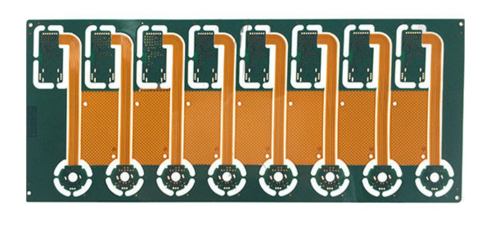
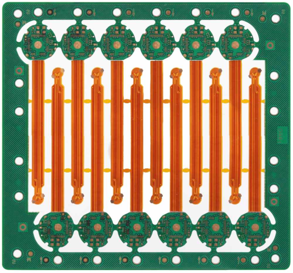
Semi rigid flex PCBs utilize a sandwich construction with alternating layers of rigid and flexible substrates bonded together. This allows the PCB to bend and flex in certain areas while maintaining rigidity in others.
The rigid portions of the PCB are made from standard rigid PCB substrates like FR-4, while the flexible portions are made from polyimide or other flexible polymer films like Kapton. conductors are etched on the flexible layers to connect the rigid regions while allowing flexing and bending.
There are a few different configurations of semi rigid flex PCBs:
Rigid-Flex-Rigid: This type has multiple rigid sections connected by flexible sections acting as hinges. The rigid regions provide mechanical stability and component mounting while the flex areas allow movement and 3D assembly.
Flex-Rigid-Flex: In this configuration, a central rigid section has flexible tails extending from both sides. The rigid segment houses components while the flex tails connect to other areas.
Rigid-Flex: Here a single main rigid section has a flexible extension coming off one side. The rigid area provides stability with the flex portion allowing a singular flexible segment.
The rigid and flexible layers are laminated together using adhesives or thermoplastics like acrylics. Aligning and bonding the layers requires precision to avoid shorts or open circuits.
Benefits and Applications of Semi Rigid Flex PCBs
Semi rigid flex PCBs provide several important advantages over traditional rigid PCBs or fully flexible PCBs:
Dynamic Flexing and Shaping: The flex regions allow the PCB to bend, twist, fold and dynamically change shape to accommodate unique device mechanics, movement or assembly. This enables new flexible form factors.
3D Assembly: Components can be assembled onto multiple rigid segments and connected via the flexible joints. This allows efficient 3D packaging and folding.
High Component Density: By folding or wrapping the flex PCB, more components can fit into a given area achieving higher density layouts.
Thinner and Lighter: Semi rigid flex PCBs with thin flexible layers reduce weight and space requirements versus rigid PCBs.
Enhanced Reliability: The flexible areas absorb stresses from motion or vibration that would break solder joints on rigid boards. This improves reliability.
Reduced Cabling: Flexible portions can replace wire harnesses or cables for simpler, more compact interconnections.
These advantages make semi rigid flex PCBs well suited for many applications including:
- Wearable electronics
- Medical devices
- Consumer electronics
- Robotics and UAVs
- Automotive electronics
- Industrial equipment
- Military/Aerospace systems
Any application where size, weight, and reliability are important considerations can benefit from the unique properties of semi rigid flex PCBs. The combination of flex and rigidity provides new design possibilities not achievable with fully rigid or fully flexible PCBs.
Design and Layout Considerations
Designing a successful semi rigid flex PCB requires careful planning of the rigid and flexible segments as well as the component placement. Here are some key guidelines for design and layout:
Plan Rigid and Flex Areas: Determine which portions of the circuit need to be rigid and flexible. Position high density components and connectors in rigid sections while lightweight traces can be routed through flex areas.
Minimize Flex Bends: Avoid sharp flex bends and use large bend radii greater than 6X the board thickness for reliability. Create chamfered corners on rigid sections.
Place Components Carefully: Ensure components are placed fully within rigid segments and not overlapping flexible areas. Watch component clearance from edges too.
Balance Layer Stacks: Maintain symmetry by balancing copper layers on either side of the neutral axis to avoid curling. Keep layer stacks consistent.
Use Flex-Friendly Parts: Select components rated for flex PCB assembly such as chip resistors or leadless packages. Avoid leaded parts.
Reduce Flex Layers: Use fewer copper layers in the flex sections to improve flexibility and prevent cracking.
Anchor Flex Ends: Anchor the ends of the flex regions to rigid sections using solder or adhesive. Prevent delamination.
Test Flexibility: Prototype and test the design to ensure the planned rigid and flex areas bend as intended without damage.
Careful design and review can help avoid common issues like fractured traces, solder cracks, or collateral damage during assembly on semi rigid flex boards.
Manufacturing and Assembly
Producing semi rigid flex PCBs requires specialized manufacturing processes beyond normal rigid PCB fabrication. Here are some of the key manufacturing steps:
Lamination: Precisely align flexible and rigid layers and use heat and adhesive films to laminate them into a bonded stackup. Avoid misalignment.
Etching: Use photolithography to image and etch the copper traces into both rigid and flexible layers. Maintain trace widths/spacing.
Folding and Shaping: Route and form drill holes to facilitate folding and shaping into 3D configurations after assembly.
Stiffener Integration: Add stiffeners around cutouts or edge fingers for increased rigidity when needed.
Solder Mask: LPI solder masks tend to perform better than liquid masks when spanning rigid-flex boundary areas.
Surface Finishes: Immersion silver provides excellent shelf life and solderability on both rigid and flex regions.
Singulation: Use router or laser cutting to singulate the boards without damaging traces in flex areas. Allow room for shifting.
Via Protection: Cover exposed flex via barrels with encapsulant or coverlay to prevent barrel cracks.
Test and Inspection: Use electrical testing and AOI to validate proper rigid-flex connections and ensure quality.
For assembly, semi rigid flex PCBs require careful component placement and mounting considerations:
- Parts should be glued or soldered only to rigid areas using flex-friendly adhesives and solders.
- Apply reinforcements like corner bonds to attach components near rigid-flex interfaces.
- Avoid placing connectors or heavy parts on flex sections to prevent damage.
- Use fixtures, jigs and clamping to prevent shifting or separation during soldering.
- Manual or secondary reflow may be required to solder complex 3D assemblies.
With attention to manufacturing and assembly requirements, semi rigid flex PCBs can be produced and assembled smoothly.
Cost Tradeoffs
While offering advantages, semi rigid flex PCBs also come with increased costs over rigid PCBs due to:
- Additional flexible substrate and adhesive/lamination materials.
- Tighter layer to layer registration and bonding requirements.
- More complex photolithography steps on different material types.
- Specialized via protection and stiffening processes.
- Precise folding, shaping and fabrication steps.
- Lower panel utilization due to irregular board geometries.
- More complex assembly requirements.
However, these costs may be offset by benefits like reduced wiring and cabling, simpler product assembly, higher reliability and performance gains. Some cost savings opportunities include:
- Using simpler flex layer stacks with fewer layers where possible.
- Standardizing designs on panel sizes optimized for utilization.
- Leveraging design for manufacturing guidelines to simplify fabrication.
- Employing design-to-cost flexibility by varying rigid vs flex amounts.
- Utilizing higher volume manufacturers with scale advantages.
- Balancing feature requirements to avoid over-engineering.
As with any PCB technology, there are always cost-performance tradeoffs to evaluate when implementing semi rigid flex designs.
Reliability Testing and Considerations
Verifying the reliability of semi rigid flex PCBs requires testing focused on the potential failure mechanisms unique to the technology:
Flexure Testing: Evaluates trace integrity, insulation robustness and functionality through the flexing cycles the design will experience.
Dynamic Bend Testing: Applies repeated dynamic bending stresses to validate robustness of the flexible regions and prevent conductor fatigue or cracking.
Peel Strength Testing: Quantifies adhesion between flexible and rigid sections to prevent interfacial separation or delamination over product lifetime.
Torsion and Twist Testing: Validates ability of the flex areas to handle twisting motions without damage during use.
Drop/Shock Testing: Tests resistance to impact damage that could occur to thinner flexible segments during drops or impacts.
Environmental Testing: Combined temperature, humidity, thermal shock helps detect issues with interfaces, adhesives, vias under use conditions.
Life Cycle Testing: Subjects the PCB to the full mechanical and environmental conditions of the product’s intended operating life.
With effective reliability testing methods, potential field failures due to improper design or manufacturing can be reduced, improving the robustness of semi rigid flex PCBs.
Frequently Asked Questions
Can semi rigid flex PCBs be double sided?
Yes, semi rigid flex PCBs can be fabricated with circuit layers on both sides of the board in either the rigid, flex or both sections. Double sided construction provides enhanced interconnection capacity compared to single sided.
How thin can the flexible sections be?
Flexible layers down to 25 microns are typical, but some specialized processes can produce 12 micron flex layers for maximum thinness. Thinner layers improve flexibility but are more prone to damage.
What density interconnects can semi rigid flex PCBs support?
Fine line processes can produce trace widths and spaces down to 4/4 mils, while microvias of 0.2mm are possible. This enables high density interconnections comparable to rigid boards.
Can traditional SMT assembly be used?
Yes, SMT assembly is regularly used for populating components on the rigid portions of semi rigid flex PCBs. However, some flex-friendly adaptations may be required.
What are typical minimum bend radii for semi rigid flex PCBs?
Most designs utilize a minimum bend radius 6-10X the total board thickness. With thinner, more advanced flex materials bend radii under 3mm are achievable.
Conclusion
Semi rigid flex PCBs provide an invaluable design option marrying the benefits of rigid and flexible PCBs into one technology. By combining rigid and flex regions, semi rigid boards can achieve smaller, lighter and more reliable electronics packaging not feasible with fully rigid PCBs.
However, realizing these advantages requires careful design, manufacturing and assembly considerations to avoid pitfalls. With an understanding of the tradeoffs involved, semi rigid flex PCBs present new opportunities for innovation across a wide range of electronic products and applications.
The future is bright for this emerging PCB technology as it enables the next generation of thinner, faster and more reliable electronic devices.