

Introduction
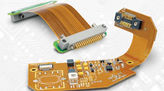
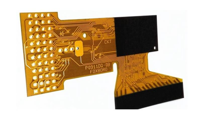
Flexible printed circuit boards (flex PCBs) are circuits built on flexible polymer substrates that can bend and flex. Multilayer flex PCBs contain two or more conductive layers separated by flexible dielectric layers. They allow complex circuitry to fit into small, dynamic packages.
Multilayer flex circuits provide several advantages over rigid PCBs or single layer flex PCBs:
Advantages of Multilayer Flex PCBs
- More compact size for complex or dense circuitry
- Flexibility and bendability for dynamic applications
- Reduce weight and 3D complexity
- Enable advanced electrical performance
- Improve reliability with fewer interconnects
- Design freedom with flexible shape and folding
Multilayer flex PCBs are commonly used in consumer electronics, medical devices, aerospace systems, and automotive applications. This guide provides a technical overview of multilayer flex PCB properties, design considerations, manufacturing processes, and applications.
Multilayer Flex PCB Properties
Multilayer flex PCBs have a layered construction with alternating conductive and dielectric layers bonded together.
Conductive Layers
The conductive layers are typically copper foil etched into circuits and traces. Flex PCBs generally use electrodeposited or rolled annealed copper foil. Electrodeposited copper has a smooth surface and tight grain structure ideal for fine features.
Common copper weights for flex PCBs range from 1⁄4 oz (8.5 μm) to 2 oz (70 μm) thickness. Heavier copper provides better conductivity and current carrying capacity. Lighter copper allows tighter bending radii.
The copper is etched into traces and covered with a thin organic surface finish for oxidation protection and solderability. Common finishes include OSP (organic solderability preservative), immersion silver, immersion tin, and ENIG (electroless nickel immersion gold).
Dielectric Layers
The dielectric layers provide electrical isolation between copper layers and allow the layers to cross over each other. The material must be thin, flexible, and thermally stable.
Typical dielectrics for multilayer flex PCBs include polyimide, polyester, PTFE composites, and liquid crystal polymer films. Polyimide films like DuPont Kapton provide an excellent balance of flexibility, temperature tolerance, and electrical performance.
Adhesives bond the dielectric layers with the copper foil layers. Thermoset adhesives like acrylic, epoxy, or polyimide are commonly used. The adhesive must withstand flexing, temperature extremes, and process chemicals.
Design Considerations
Several factors go into designing an optimal multilayer flex PCB:
Layer Stackup
The sequence and thickness of the conductive, adhesive, and dielectric layers impacts flexibility, electrical performance, manufacturability, and cost. Common multilayer constructions utilize 2-8 conductive layers.
Bend Radius
A primary design factor is the minimum bend radius the PCB can tolerate without damage. Smaller bend radii allow tighter folding but require thinner dielectrics. Bend radius depends on copper thickness, dielectric material, layers used, and applied stresses.
Conductor Spacing and Routing
Multilayer flex PCBs support tighter conductor spacing and higher routing densities than rigid PCBs. Typical trace/space is 100 μm (4 mils) with capability down to 50 μm (2 mils). Thinner dielectrics and copper allow even finer lines and spaces.
Stiffeners and Shielding
localized stiffeners may be added for components or connectors. Shielding layers can provide EMI protection. Stiffeners and shields impact flexibility in those regions.
High-Frequency Performance
Matching impedances, minimizing crosstalk, and controlling signal speeds are necessary for RF or high-speed design. Thin dielectrics with higher performance materials are used.
Manufacturing Process
Multilayer flex PCBs require specialized fabrication processes to create the multilayer construction and fine features.
Layer Fabrication
Conductive and dielectric layers are fabricated separately. Copper layers undergo photolithographic processing and etching to form the traces and features. Dielectric films are cut to size. Layers are cleaned and prepared.
Layer Bonding
The layers are precisely aligned and bonded together under heat and pressure. The adhesive cures to form a permanent bond. Registration accuracy is critical for vias lining up between layers.
Via Formation
Mechanically drilled or laser drilled holes are used to create the vertical interconnects between layers. The holes are plated with copper to form the via barrel. Exposed copper is coated with surface finish.
Solder Mask
Solder mask is applied over the surface for soldering protection. Areas are opened for soldering pads and connections. Flex PCBs typically use liquid photoimageable solder mask.
Final PCB Processing
Final processing and testing complete the boards. This includes electrical testing, singulation from panels, and quality inspection.
Applications
The unique properties of multilayer flex PCBs make them ideal for many advanced applications.
Consumer Electronics
Multilayer flex is used extensively in mobile phones, laptops, tablets, cameras, watches, and other compact interconnect applications. The dynamic flexing and folding requirements favor multilayer flex PCBs over rigid technology.
Medical Devices
Medical electronics like hearing aids, health monitors, and sensors integrate multilayer flex PCBs. The small, lightweight circuits can conform to the body.
Automotive Electronics
In automotive applications, multilayer flex PCBs handle vibration while fitting into tight spaces. Flex PCBs are used in dashboard displays, engine controls, sensors, and entertainment systems.
Aerospace and Defense
Multilayer flex provides lightweight, rugged interconnects for aerospace systems. The boards withstand vibration while minimizing weight. Applications include guidance systems, engine controls, communications, and navigation electronics.
Wearable Technology
For smart clothing or wearable devices, multilayer flex PCBs can conform to clothing and body movement. The bendable PCBs connect components in a lightweight, comfortable product.
Multilayer Flex PCB FAQ
What are the typical dielectric materials used in multilayer flex PCBs?
The most common dielectrics are polyimide films (Kapton), polyester (PET), PTFE composites, and liquid crystal polymer (LCP). Polyimide provides the best all-around flexibility, thermal stability and electrical performance.
What are some typical ways multilayer flex PCBs are used in consumer electronics?
In mobile phones, multilayer flex is used for displays, cameras, button interconnects, and folding or hinging mechanisms. In laptops, flex PCBs connect the base to the display. Other uses include digital cameras, wearable devices, game controllers, and virtual reality systems.
How many conductive layers can flex PCBs support?
While 2-6 layers are typical, advanced designs use up to 12 conductive layers or more by utilizing thinner dielectric films. As layer count increases, minimum bend radius and overall stiffness increase as well.
How are components attached to multilayer flex PCBs?
Common component attachment methods include soldering, conductive epoxy, and mechanical fasteners. Softboard connectors allow removable mating between rigid PCBs. Special flex-friendly components are also produced.
How is impedance controlled on multilayer flex PCBs?
For controlled impedance on high-speed multilayer flex PCBs, trace geometry is the primary method. Thin dielectrics improve impedance precision. Some flex materials allow microstrip lines or grounded coplanar waveguides.
This concludes the overview on multilayer flex PCB technology. Let me know if you would like me to modify or expand this article draft in any way. I can incorporate additional details, technical examples, images, or applications focused on your target audience.