

Introduction
Rigid-flex printed circuit boards (PCBs) combine rigid and flexible substrates to create lightweight, robust electronic devices that can fit into tight spaces. Rigid-flex allows designers to install electronic components in multiple rigid areas connected through flexible circuits that can bend and twist. This enables more compact and ergonomic designs for products like smartphones, wearables, medical devices, and more.
Altium Designer provides designers with powerful tools to easily create complex rigid-flex designs. In this guide, we will explore key considerations and features in Altium for designing and manufacturing rigid-flex PCBs.
Designing Rigid-Flex with Altium
When designing rigid-flex PCBs in Altium, there are some important factors to consider:
- Materials – Rigid material like FR4 combined with flexible material like polyimide film. The materials must be well-bonded.
- Layer stackup – The sequence and thickness of the conductive and dielectric layers.
- Bends – Minimizing stress on traces routed across bends. Controlled bend radius.
- Transitions between rigid and flex – Preventing failures between different board stiffness.
- Component placement – Strategic placement for space and routability.
- Routing – Difficult connections may require fanout or bridging.
Altium provides design features and rules assistance tailored to rigid-flex, like:
- Defining flex and rigid sections on the same PCB document.
- Layer stack manager for the layer structure.
- Enhanced high-speed and length-matching routing capabilities.
- Rigid-to-flex transitions with controlled teardrops.
- 3D PCB editor and MCAD collaboration.
- Manufacturing documentation like guides and notches.
With the right design approach, components and routing can be optimized in both the rigid and flexible regions of the board.
Rigid-Flex Design Steps in Altium
Here is an overview of the typical workflow when designing rigid-flex PCBs in Altium Designer:
- Define rigid and flexible regions – separate mechanical sections.
- Choose a layer stackup – often 1 or 2 conductive layers on flex.
- Assign materials to regions – FR4 for rigid, polyimide for flex.
- Add components – mindful of rigid vs flex placement.
- Create the tracks – with routing awareness of materials.
- Add rigid-flex transitions – teardrops to ease stresses.
- Validate the 3D design – check clearance, tolerances.
- Generate manufacturing files.
Rigid-Flex Rules
Altium includes built-in design rule checking (DRC) specifically for rigid-flex PCB constraints like:
- Flex bend radius – avoid overstressing flex areas.
- Rigid-to-flex transitions – control teardrops and spacing.
- Annular rings – ensure pad integrity on flex areas.
- SMT pad spans – check spacing and solder mask squeeze.
The rules generator helps set appropriate spacing and sizing needs for a reliable rigid-flex design.
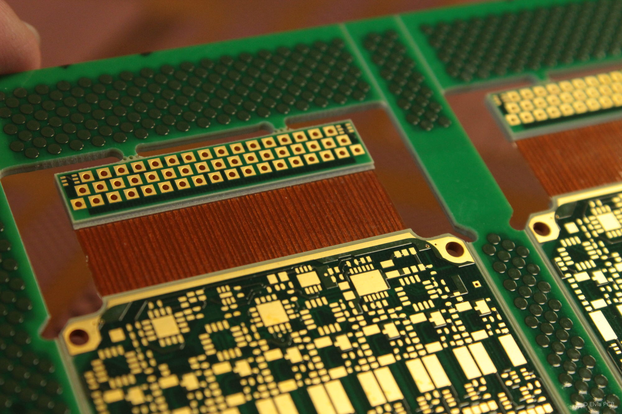
Rigid-Flex Layer Stackup Considerations
Careful planning of the layer stackup is a key part of rigid-flex PCB design in Altium.
For the rigid sections, a typical 4-layer or more stackup can allow for adequate component placement, routing channels, and circuit density.
The flexible sections are often limited to 1 or 2 conductive layers to reduce thickness and retain flexibility. An example 2-layer flex stackup:
- Layer 1 – Coverlay
- Layer 2 – Signal traces
- Layer 3 – Dielectric film core
- Layer 4 – Signal traces
- Layer 5 – Stiffener
Here are some layer stackup guidelines for rigid-flex:
- Keep flex layers to 1-2 conductors to avoid stiffening from excessive copper thickness.
- Ensure bondply layers adhere the rigid and flex materials through lamination.
- Add protective coverlay layers on the top and bottom of the flex layer package.
- Include a stiffener layer on the external side of flex to prevent flexing of components.
- Allow for generous vertical spacing between conductors to prevent shorts through the flex.
Altium’s layer stack manager lets designers configure the different layer sequences in rigid and flex zones to achieve a robust, manufacturable layer stackup.
Working With Rigid-Flex Bends
A core design consideration for rigid-flex is the bending sections where the thin flexible circuits transition between rigid regions.
Here are some best practices for working with bends:
- Minimize the number of bends to reduce stress and complexity. Allow plenty of room for full bend radiuses.
- Avoid routing traces perpendicular to the bend axis as it exposes them to tear-out stress. Route parallel or at 45 degree angles.
- Place components near the neutral bend axis whenever possible, rather than near the peak stresses at the outer surfaces.
- Add teardrop pads at bends to reduce sharp angle stresses. Larger pad diameters give more margin against failure.
- Leave generous spacing between conductors routed across bends to prevent shorting through the flexible material when bent.
Altium provides features like teardrops, spacing checks, and DRC rules to help designers account for rigid-flex bend requirements.
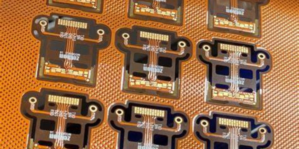
Transitions Between Rigid and Flexible
The intersections between rigid and flexible sections demand special attention to reduce mechanical stresses that can lift pads or tear traces.
Here are some ways to smoothen rigid-to-flex transitions in Altium:
- Use teardrops to spread stresses at junctions between materials with different stiffness.
- Bevel the edges of the rigid board at transitions using smooth curves instead of sharp corners.
- Include stop mask layers to provide barriers that prevent tear propagation.
- Add slots in the rigid sections next to junctions so flexing does not stress attachments.
- Provide sufficient clearances between conductors crossing transitions.
Rigid-flex design rules in Altium will help identify potential issues at rigid/flex transitions that require pad and trace adjustments. This ensures the PCB can withstand reasonable flexing.
Placing Components and Routing in Rigid-Flex
PCB features need to be arranged differently between the sections of a rigid-flex design in Altium.
For component placement:
- Dense, tightly packed SMT parts should go in rigid sections while flex areas use minimal, smaller components.
- Place components along the neutral bend axis when possible, rather than near the high-stress outer surfaces.
- Ensure clearance from edges of rigid sections into bend areas.
- Watch component orientation so leads are routed appropriately.
Routing considerations include:
- Use vias and through holes sparingly on flex areas due to punching/drilling challenges.
- Route critical signals across flex parallel to bend axis, not perpendicular.
- Minimize trace density across bends to lower chances of shorting.
- Extend traces fully across flex sections, avoiding stubs.
- Allow for substantial spacing between traces when crossing bends.
Altium’s rigid-flex routing modes help guide trace paths across different sections and materials while obeying clearance rules.
Rigid-Flex PCB Manufacturing Notes
Compared to standard rigid PCBs, rigid-flex boards can present additional manufacturing challenges. Designers should account for fabrication needs.
Some suggestions include:
- Add reference holes for tooling/alignment of layers.
- Use communication cutouts on interior layers to indicate panel sections.
- Include assembly fixtures like jigs or rails to support boards during population.
- Note special hole punch/drilling requirements for flex vias. May need different bits.
- List the target bend radius and note critical dimensions.
- Provide layered board images for laminating visualization.
Clear manufacturing documentation will support a smooth rigid-flex board fabrication process.
Conclusion
Altium Designer provides smart tools to manage the intricacies of advanced rigid-flex PCB designs. Using the specialized features for rigid-flex materials, constraints, and transitions helps set designers up for manufacturable, functional boards. Rigid-flex opens new possibilities in electronic product design.
Resources
- Altium Academy Course on Rigid-Flex Design
- Altium Techdoc on Rigid-Flex Design Standards
- Rigid-Flex Materials and Construction Guide
FAQ
What are the benefits of a rigid-flex PCB?
Rigid-flex PCBs offer several advantages over rigid boards:
- More compact and ergonomic designs by folding rigid sections connected by flex circuits.
- Ability to fit PCBs into tight spaces that rigid boards won’t fit.
- Withstands vibration/shock better by absorbing stresses across flex areas.
- Allows creative industrial design and packaging options.
- Lightweight compared to rigid solutions due to need for less material.
What types of products use rigid-flex PCBs?
Common applications include:
- Mobile consumer electronics like cell phones and wearables.
- Internet of things and other small connected devices.
- Medical instruments with tight space requirements.
- Military and aerospace systems with high vibration/shock needs.
- Automotive electronics demanding flexibility and reliability.
What are considerations for the rigid vs flex areas?
- Rigid sections can support more densely packed components and multilayer circuitry.
- Flex sections should minimize component density, traces, and layers.
- Take care in component placement between rigid and flex zones.
- Account for different routing and spacing needs between sections.
How do rigid and flex sections interconnect?
Connections require careful design at the junctions:
- Use teardrops and beveled edges to reduce mechanical strain.
- Allow sufficient trace clearance across junctions.
- Route traces parallel, not perpendicular, to bend axis.
- Add protective stop mask layers to prevent tear propagation.
What fabrication notes help manufacture rigid-flex?
Include notes on:
- Target bend radius for flex zones.
- Holes/vias that require special drilling or punching.
- Fixture and tooling needs for assembly.
- Panel sections and breakout information.
- Visuals of layer stackup.