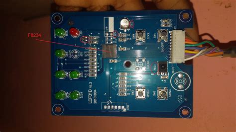
PCB Substrate
The substrate is the foundation of the PCB, providing a rigid base for the other components to be built upon. The most common substrate materials are:
FR-4
FR-4 is a glass-reinforced epoxy laminate that is widely used in the electronics industry. It offers good mechanical strength, electrical insulation, and heat resistance. FR-4 is composed of multiple layers of glass cloth impregnated with epoxy resin, which are then cured under heat and pressure to form a solid board.
CEM-1 and CEM-3
CEM (Composite Epoxy Material) is another popular substrate choice for PCBs. CEM-1 is made of a combination of woven glass cloth and paper, while CEM-3 uses only woven glass cloth. These materials offer similar properties to FR-4 but at a lower cost, making them suitable for less demanding applications.
Polyimide
Polyimide is a high-performance substrate material that offers excellent thermal stability, chemical resistance, and mechanical strength. It is often used in applications that require the PCB to withstand extreme temperatures or harsh environments, such as in aerospace or military equipment.
Copper Foil
Copper foil is the conductive layer of the PCB, responsible for carrying electrical signals between components. It is typically laminated onto the substrate using heat and pressure. The thickness of the copper foil is measured in ounces per square foot (oz/ft²), with common thicknesses ranging from 0.5 oz/ft² to 2 oz/ft².
The copper foil is usually electrodeposited (ED) or rolled annealed (RA). ED copper is created by electroplating copper onto a drum, resulting in a smooth, shiny surface. RA copper is made by rolling copper sheets under high pressure, creating a matte finish with better adhesion to the substrate.
Solder Mask
The solder mask is a protective layer applied to the surface of the PCB, covering the copper traces while leaving the pads and other areas that require soldering exposed. Its primary purpose is to prevent Solder Bridges from forming between adjacent traces during the soldering process. Solder mask also provides insulation and protection against oxidation and environmental factors.
Solder mask is typically made of a photoimageable polymer that is applied as a liquid and then cured using UV light. The most common Solder Mask Colors are green and blue, but other colors such as red, yellow, and black are also available.

Silkscreen
Silkscreen, also known as legend or nomenclature, is a layer of text and symbols printed onto the surface of the PCB. It is used to identify components, provide assembly instructions, and display company logos or other branding elements. Silkscreen is typically printed using a white or yellow ink, although other colors are available for special applications.
The silkscreen layer is usually the last to be applied to the PCB, after the solder mask has been cured. It is important to ensure that the silkscreen does not overlap with any pads or other areas that require soldering, as this can interfere with the assembly process.
Surface Finish
The surface finish is a thin layer of metal applied to the exposed copper pads and other areas of the PCB that require soldering. Its purpose is to protect the copper from oxidation and improve solderability. There are several common surface finishes used in PCB manufacturing:
HASL (Hot Air Solder Leveling)
HASL is a widely used surface finish that involves dipping the PCB in molten solder and then using hot air to level the surface. This creates a thin layer of solder on the exposed copper, providing good protection against oxidation and excellent solderability. However, HASL can result in an uneven surface and is not suitable for fine-pitch components.
ENIG (Electroless Nickel Immersion Gold)
ENIG is a two-layer surface finish that consists of a nickel layer deposited on the copper, followed by a thin layer of gold. The nickel provides a barrier against copper diffusion, while the gold offers excellent solderability and protection against oxidation. ENIG is suitable for fine-pitch components and has a long shelf life, making it a popular choice for high-reliability applications.
OSP (Organic Solderability Preservative)
OSP is a thin, organic coating applied to the exposed copper to protect it from oxidation. It is a low-cost alternative to metallic surface finishes and is often used in applications where the PCB will be assembled shortly after manufacturing. OSP has a limited shelf life and may not be suitable for high-temperature or multiple reflow cycles.
Vias
Vias are conductive pathways that connect different layers of a multi-layer PCB. They are created by drilling holes through the substrate and plating them with copper. There are several types of vias used in PCB Design:
Through-hole Vias
Through-hole vias are the most common type, extending from the top layer to the bottom layer of the PCB. They are used to connect components mounted on opposite sides of the board or to provide electrical connections between layers.
Blind Vias
Blind vias are used to connect an outer layer to an inner layer of the PCB, without extending through the entire board. They are typically used to save space and improve signal integrity in high-density designs.
Buried Vias
Buried vias are used to connect two or more inner layers of the PCB, without extending to either of the outer layers. They are used to create complex interconnections within the board and are often found in high-performance applications.
FAQ
1. What is the most common substrate material used in PCBs?
FR-4 is the most widely used substrate material in the electronics industry, offering a good balance of mechanical, electrical, and thermal properties.
2. What is the purpose of the solder mask on a PCB?
The solder mask is a protective layer that covers the copper traces on the PCB, preventing solder bridges from forming between adjacent traces during the soldering process. It also provides insulation and protection against oxidation and environmental factors.
3. What is the difference between ED and RA copper foil?
ED (electrodeposited) copper foil is created by electroplating copper onto a drum, resulting in a smooth, shiny surface. RA (rolled annealed) copper foil is made by rolling copper sheets under high pressure, creating a matte finish with better adhesion to the substrate.
4. What are the most common surface finishes used in PCB manufacturing?
The most common surface finishes are HASL (Hot Air Solder Leveling), ENIG (Electroless Nickel Immersion Gold), and OSP (Organic Solderability Preservative). Each offers different advantages in terms of solderability, protection against oxidation, and suitability for fine-pitch components.
5. What are vias, and what types are used in PCB design?
Vias are conductive pathways that connect different layers of a multi-layer PCB. The most common types are through-hole vias (connecting top to bottom layer), blind vias (connecting an outer layer to an inner layer), and buried vias (connecting two or more inner layers without extending to the outer layers).
In conclusion, PCBs are complex assemblies made up of several basic components, each of which contributes to the overall functionality and reliability of the final product. By understanding the properties and roles of these materials, designers and manufacturers can create PCBs that meet the specific requirements of their applications, ensuring optimal performance and longevity.


