


What Is the Difference Between PCBA and PCB?
Introduction to PCBA and PCB
PCBA stands for Printed Circuit Board Assembly while PCB stands for Printed Circuit Board. Though they sound quite similar and are closely related, there are some key differences between the two.
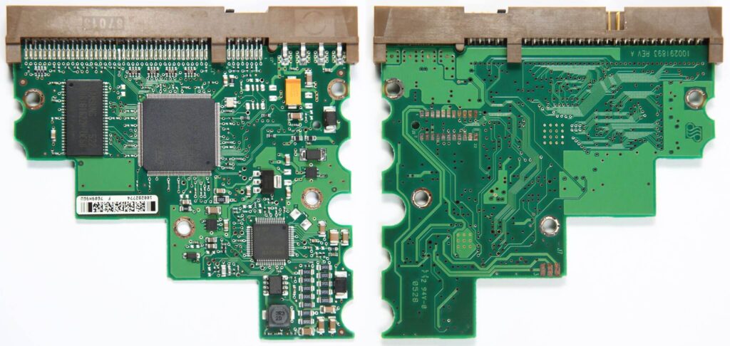
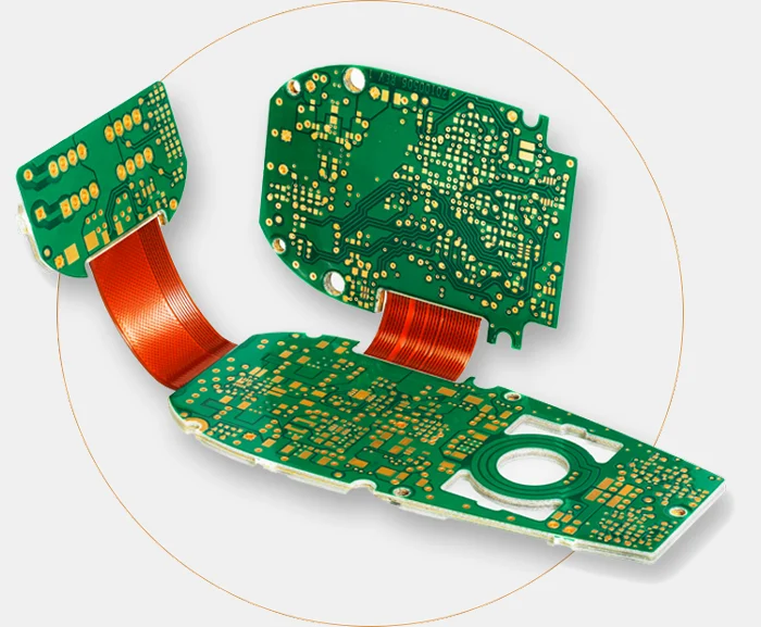
A PCB refers specifically to the bare circuit board before any components have been soldered to it. A PCBA refers to a PCB that has had electronic components soldered to the board. In essence, PCBA would be considered the complete, functioning circuit board assembly.
Key Characteristics of a PCB
A PCB starts out as a flat piece of fiberglass or composite material used to mount and connect electronic components. Here are some of the key characteristics of a typical bare PCB:
- Laminated sheet made of fiberglass, composite, or other material
- Copper tracing etched onto one or both sides
- Holes and pads for inserting and soldering components
- May have silkscreen labelling and markings
- Protective soldermask layer over copper
PCBs provide the foundation for building functioning electronic devices and products. But on their own, they do not do anything until components get populated onto them.
What Constitutes a Complete PCBA?
A PCBA refers to a PCB that has been fully assembled and populated with electronics components. This would include key elements like:
- A working PCB substrate as described above
- Soldered components like resistors, capacitors, ICs, processors etc.
- Any connectors, switches, or other addons to aid functionality
- Often an enclosure or case the assembly is mounted into
- May have attached firmware loaded onto memory
- Fully functioning electronic circuit able to perform designed tasks
So in summary, the key difference is that a PCB is a bare circuit board, while a PCBA has all required components loaded onto the PCB to do its job.
Comparing Design, Production and Testing
There are some clear differences when comparing the design, production, and testing phases between bare PCBs and finished PCB assemblies:
PCB Design vs PCBA Design
PCB Design
- Focus is on physical board itself
- Layout of traces, pads, holes
- Getting board layers correctly setup
- Planning part placements locations
- Finalizing overall board dimensions
PCBA Design
- Includes PCB design
- Additional focus on components selection
- Ensuring parts will correctly fit and orient
- Designing any necessary sub-assemblies
- Planning production process steps
So PCBA design builds on PCB design, accounting for component choices and manufacturing requirements for loading a functioning assembly.
PCB Production vs PCBA Production
PCB Production
- About physically manufacturing bare PCB
- Steps like lamination, etching, drilling
- Specialized PCB fabrication setups
- Output is bare PCB ready for population
PCBA Production
- Starts with bare PCB
- Done at electronics manufacturing facility
- May have SMT line to automate loading
- Manual soldering stations also possible
- Additional inspection and testing stages
PCB production represents just the first phase of the overall journey, providing a blank slate ready to build the full PCBA on.
Testing Bare PCBs vs Testing PCBA
PCB Testing
- Verifying bare board meets design
- Using tools like optical inspection
- Automated testing for opens/shorts
- Checking for internal layer misalignments
- Validates quality before populating
PCBA Testing
- Includes PCB tests
- Plus total functionality testing
- Running self-diagnostics if available
- Stress testing over temp/voltage ranges
- Final check assembly works correctly
PCBA testing not only checks the board itself but all loaded components too. The end deliverable must be completely validated before shipping finished product.
Cost Comparison of PCB and PCBA
There can be considerable cost differences between procuring bare PCB boards vs complete functioning assemblies:
| Assembly Item | Typical Cost |
|---|---|
| 2 Layer PCB | $5 to $100+ |
| 4-6 Layer PCB | $50 to $5,000+ |
| 8+ Layer HDI PCB | $500 to $50,000+ |
| SMT Assembly | $100 to $10,000+ per project |
| Manual Soldering | $$ per hour |
| Component Costs | Wide cost ranges |
| Lead Times | PCBs: 2-4 weeks, PCAs 4-8+ weeks |
In general, and not surprisingly, a PCBA with loaded functionality can cost anywhere from 10-100X+ the cost of the raw PCB substrate itself. Main drivers come down to:
PCB Cost Drivers
- Board dimensions
- Layer count
- Advanced PCB technologies
PCBA Cost Drivers
- Component selection/Bom Bill of Materials
- Lead times for ICs/chips
- Assembly method (automated vs manual)
- Test requirements
- Certifications
- Production quantities
For low complexity boards with cheaper components, the differential may lower end of range. But for advanced products with sophisticated ICs, assembly can be main expense.
This also translates into longer fabrication lead times once including PCBA steps, over just basic PCB production alone.
Choosing PCB Only or Full PCBA Services
Given the comparison points covered above, when does it make sense go with a bare PCB board versus a complete PCBA assembly during product development?
Here are some factors to consider:
When PCB Only Approach Works
- If limited electronics design expertise
- When access to component loading and debugging
- For testing out board viability early
- Allows iteratively improving layouts as needed
When Full PCBA Approach Preferred
- Want turnkey product development
- To enable rapid prototyping
- Have reliable assembly vendor/factory
- Component sourcing complexities
- To reduce project development/validation timeline
For quick validation of a PCB layout itself, procuring bare boards can offer flexibility. But for complete functioning prototypes or production rollouts, having an expert assembly partner handle PCBA is preferred.
Hybrid Approaches
A mixed strategy is also possible when priorities evolve over the project development and rollout roadmap from concept to mass production.
Frequently Asked Questions
What are the layers in PCB?
The layers in a PCB refer to the stackup of the circuit board itself. Simple PCBs often consist of just two copper layers—a top and bottom layer. More complex designs can incorporate 6, 8, or more layers laminated together allowing routing between layers. Typical layer counts include:
- 2-Layer one top side and one bottom side
- 4-Layer two inner layers and top/bottom sides
- 6-Layer four inner layers
- 8+ Layer high density interconnect boards
Are PCB and PCBA the same?
No, PCB and PCA are not the same. As covered in this article:
- PCB refers specifically to the bare printed circuit board, consisting of an insulating substrate made out of fiberglass or composite materials that forms the foundation
- PCBA then refers to a PCB that has had electronic components soldered directly to pads on the PCB substrate to create a functioning electronic printed circuit assembly
So in summary:
- PCB = Blank circuit board without components
- PCBA = Circuit board with components soldered directly onto it
They are closely related but distinct electronics hardware artifacts.
Why use PCBA over a PCB?
There are several reasons why it typically makes sense to use a complete PCBA over simply using a bare PCB:
Benefits of Using PCBA
- Saves on development time versus self-assembly
- Leverages assembly partner experience
- Avoid specialist equipment like SMT lines
- Eliminates risky hand soldering of complex ICs
- Higher reliability with inspection/testing
- Faster time to market overall
For most types of products, leveraging a qualified contract assembly manufacturer delivers better results than attempting self-assembly. They offer specialized services, reduce project development risk, avoid equipment costs, and enable faster rollout.
What does a PCBA Design or Test Engineer do?
Those involved in PCBA-specific design/test engineering play various important roles across the printed circuit assembly development and production cycle:
Key PCBA Design Engineering Tasks
- Create schematics/layouts for circuit card assemblies
- Develop detailed BOMs Bills of Materials
- Help assess best assembly methods
- Model designs digitally and simulate operation
- Work on design-for-manufacturing requirements
Key PCBA Test Engineering Tasks
- Create test plans/procedures for assemblies
- Implement testbenches to validate PCBA builds
- Identify faults through testing and debug
- Analyze issues and offer corrective recommendations
- Validate robustness over voltage, temp, cycles
- Sign-off on assembly viability
What tools are used to test PCBAs?
A variety of specialized tools are leveraged to validate printed circuit board assemblies once manufactured:
Common PCBA Testing Tools
- Flying Probe Testers: Checks shorts, opens, impedance
- Bed of Nails Testers: Makes contact at test points
- IC Test Clips: Stimulate/probe individual ICs
- In-Circuit Testers: Validate components on board
- Automated Optical Inspection: Verify assembly accuracy
- X-Ray Inspection: Look for hidden defects/voids
A combination of different testing approaches helps fully qualify PCBA production builds.
So in summary, while PCBs set the stage, PCAs represent the final act—bringing together the full functionality called for in the initial product electronics designs. Understanding these key differences between the two drives smart engineering decisions and gets products from concept to reality smoothly.