


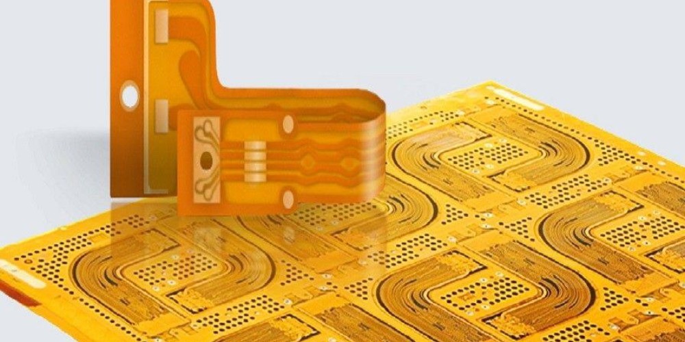
Introduction to Rigid Flex PCBs
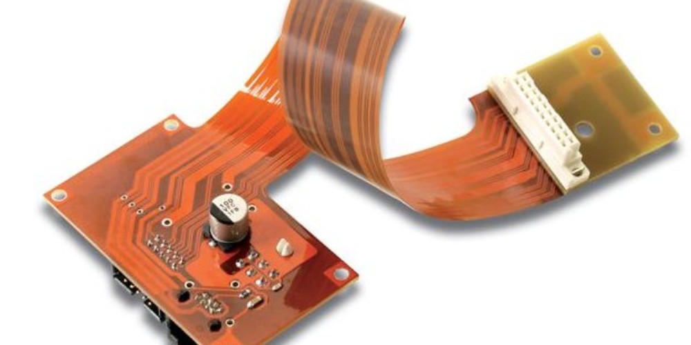
A rigid flex PCB (also known as rigid-flex circuit board) combines rigid PCBs and flexible PCB technologies into one circuit board. Rigid flex PCBs contain both rigid sections and flexible sections interconnected with laminated copper traces. The rigid sections provide mechanical support while the flexible sections allow dynamic flexing, bending or twisting.
Rigid flex PCBs provide solutions for complex and compact electronic designs where reliability and high performance are critical. They are commonly used in aerospace, defense, medical devices, industrial equipment and consumer electronics. The combination of rigid and flexible materials in one PCB allows for improved reliability, reduced system size and weight, and design flexibility.
Advantages of Rigid Flex PCBs
Here are some of the key benefits that rigid flex PCBs offer:
- Space savings: By folding and bending, rigid flex PCBs can fit into tight spaces and complex shapes. This helps reduce the overall footprint of electronic devices.
- Reliability: The bonds between the rigid and flexible sections are very durable. Rigid flex PCBs also reduce the need for connectors and cables which are often failure points.
- Flexibility: Both physically and in terms of design flexibility. Rigid flex allows three-dimensional configuration and dynamic flexing which enables innovation.
- Weight reduction: By consolidating rigid and flex PCBs into one board, overall weight is reduced compared to using separate PCBs.
- Improved High Speed Performance: The continuous electrical paths minimize impedance discontinuities and allow for higher frequency signals.
- Reduced Assembling Costs: Assembling onto one rigid flex PCB is cheaper compared to connecting separate rigid and flex PCBs.
Applications of Rigid Flex PCBs
Here are some common applications that benefit from using rigid flex PCB technology:
- Aerospace: Used in guidance systems, avionics, satellites and spacecraft. Rigid flex PCBs withstand vibration, shock and extreme temperatures.
- Medical: Used in hearing aids, patient monitoring systems, surgical equipment and other devices where reliability, size and flexibility are important.
- Consumer Electronics: Ideal for wearable devices, mobile phones, laptops, cameras and other portable gadgets where thin and light designs are valued.
- Automotive: Used in sensors, engine control units, car navigation systems, anti-lock braking systems and entertainment units.
- Industrial: Used in robotics, instrumentation, control systems, motors, pumps, and heavy machinery operating in harsh environments.
- Military/Defense: Used in guidance systems, communications, weapon systems, and body-worn electronics which require reliability and durability.
Rigid Flex PCB Construction
Rigid flex PCBs integrate flexible printed circuits and rigid printed circuits into a single assembly. Here are the key construction elements:
Laminate Materials
The rigid sections of the PCB use standard FR-4 glass epoxy substrate. FR-4 provides mechanical strength and stability for components and is suitable for most common consumer and industrial applications.
The flexible sections use polyimide film substrate such as Kapton or UPILEX. These plastic films can withstand continuous dynamic flexing over a long lifetime. Typical thicknesses range from 25μm to 75μm. Thin flexible sections allow tight bend radii.
Copper Traces
The conductive copper traces are etched onto both sides of the laminate substrate. Traces run continuously between both rigid and flexible sections. For flexible sections, the traces need to be designed as strain relief loops to withstand dynamic bending without cracking.
Coverlay/Solder Mask
A solder mask coating is applied over the copper traces for protection against oxidation and electrical shorts. For flexible sections, a polyimide coverlay is laminated on top of the copper to provide insulation and prevent tears during bending.
Stiffeners
Optionally, rigid stiffeners made from aluminum or FR-4 can be added to strengthen the flex-to-rigid transitions and prevent stresses from concentrating in one area. Stiffeners help absorb forces during flexing to improve reliability.
Vias
Vias or plated through holes electrically connect traces between layers in multilayer rigid flex boards. Special care is taken to reinforce vias in the flex-to-rigid interface regions.
Adhesives
Bonding films are used to laminate together the rigid and flex materials into one cohesive circuit board. The rigid and flex sections adhere together while allowing dynamic flexing at the joints.
Rigid Flex PCB Design Guidelines
Careful design is required to create durable and functional rigid flex PCBs. Here are some best practice design guidelines:
- Minimize rigid sections protruding from the edges of flex sections to reduce peel stresses.
- Avoid sharp 90 degree angles between rigid and flex. Use rounded corners instead.
- Design strain relief curves for traces crossing from rigid to flex rather than right angles.
- Use teardrop pads for traces at flex-to-rigid interfaces to reduce stress concentrations.
- Add stiffeners and/or adhesive to strengthen the transitions between rigid and flex.
- Ensure minimum bend radius is adhered to avoid trace cracking and damage.
- Verify board thickness change does not impact components or electrical connections.
- Run traces perpendicular to bend axis and space them evenly to distribute strain uniformly.
- Keep high-frequency traces short and uninterrupted to minimize impedance discontinuities.
Proper design is a balance between reliability, functionality, manufacturability and cost. Work closely with your PCB manufacturer during design to ensure an optimal rigid flex board layout.
Manufacturing Processes
Rigid flex PCBs require specialized fabrication processes to create durable integrating between the dissimilar substrate materials. Here are some key manufacturing steps:
Layer Preparation
The individual rigid and flexible layers are processed first to prepare them for lamination. This includes cleaning, surface treatments, dielectric coating and metallization.
Lamination
The adhesive bonding films are added and the material layers are stacked up. The multilayer board “book” goes through a high temperature and pressure lamination press. The elevated temperature cures the adhesive to form permanent bonds.
Drilling
The rigid and flex sections are drilled together using NC precision drilling machines. Smaller holes may be laser drilled. Plating is done to create the barrel vias electrically connecting the layers.
Patterning
Conventional lithographic processes are used to image the copper traces from the base copper foil onto both rigid and flexible sections. This includes photoresist coating, UV exposure, developing, etching and stripping.
Coverlay and Solder Mask
Polyimide coverlay films are laminated onto the flex sections while liquid solder mask is applied on the rigid areas. Openings are made over component pads and connections.
Testing and Inspection
Each completed rigid flex PCB is checked for defects using AOIs, x-ray inspection and electrical testing. This verifies all traces, connections and function as designed.
Assembly
Components can be assembled onto the board using standard SMT and through-hole soldering processes. Additional staking adhesives may be used to strengthen component attachments in high vibration environments.
Frequently Asked Questions
Here are some common FAQs about rigid flex PCBs:
What are the typical rigid-to-flex ratios used?
Typical rigid-to-flex ratios range from 50/50 to 80/20. A higher proportion of rigid area provides more structural support while more flex allows greater dynamic movement range. The optimal ratio depends on the application and design constraints.
What are the minimum bend radii and trace widths supported?
Minimum bend radii range from 2 to 10 mm depending on the flex material thickness. Minimum trace widths and spacing is around 4-5 mil (0.1 mm) but finer geometries are achievable with advanced processes.
How many flex/rigid layers can be accommodated?
Rigid flex PCBs typically support 4-8 total layers (including inner and outer layers). More advanced designs up to 12-14 layers are also possible. The number of layers is limited by the laminating and drilling processes.
What types of materials can be used?
FR-4, Rogers, polyimides like Kapton, and adhesive films like acrylic or epoxy are commonly used. Other exotic substrates like liquid crystal polymer (LCP) can also be leveraged for specialized applications.
How small or large can rigid flex PCBs be fabricated?
Rigid flex PCB sizes can range from under 1 inch square to over 3 feet in length or width. The maximum size is limited by the equipment capacity while the minimum depends on handling complexity. Sizes under 0.5″ can be challenging in high volume.
How are components assembled onto rigid flex boards?
SMT, COB, and press-fit technologies allow assembly directly onto the PCB as with normal rigid PCBs. For through-hole parts, clinching or adhesives help strengthen the joints to avoid cracking during flexing.
Conclusion
Rigid flex PCB technology provides the ideal solution for many modern electronics needing compact, lightweight and reliable circuitry. By combining sturdy rigid sections and dynamic flexible sections into one circuit board, rigid flex PCBs open new possibilities in design and functionality. With careful layout and assembly, components can be integrated into very small spaces while withstanding mechanical stresses. As electronic devices continue getting more powerful and compact, rigid flex PCBs will take on an increasing important role with their unique set of advantages.