


Introduction to Copper-Clad Laminate
Copper-clad laminate (CCL) is a fundamental material used in the production of printed circuit boards (PCBs). It consists of a thin layer of Copper Foil bonded to a dielectric substrate, such as fiberglass, epoxy resin, or polyimide. The combination of conductive copper and insulating substrate makes CCL an ideal foundation for creating the complex electrical circuits found in modern electronic devices.
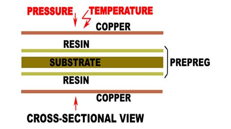
Composition of Copper-Clad Laminate
Copper-clad laminate is composed of three main components:
- Copper foil: A thin layer of pure copper, typically ranging from 9 to 180 microns (μm) in thickness. The copper foil provides the conductive pathways for electrical signals.
- Dielectric substrate: An insulating material that supports the copper foil and provides electrical isolation between different layers of the PCB. Common substrates include:
- FR-4: A glass-reinforced epoxy laminate, widely used for its excellent mechanical and electrical properties.
- Polyimide: A high-temperature resistant polymer, used in applications that require greater thermal stability.
- CEM-1 and CEM-3: Composite epoxy materials, offering a lower-cost alternative to FR-4.
- Bonding agent: An adhesive layer that ensures a strong bond between the copper foil and the dielectric substrate. The bonding agent helps to prevent delamination and maintain the integrity of the PCB.
Manufacturing Process of Copper-Clad Laminate
The production of copper-clad laminate involves several key steps:
- Substrate preparation: The dielectric substrate is cut to the desired size and shape, and its surface is cleaned and treated to promote adhesion.
- Copper foil preparation: The copper foil is also cut to size and cleaned to remove any contaminants that may affect the bonding process.
- Lamination: The prepared copper foil and dielectric substrate are sandwiched together with the bonding agent and subjected to high pressure and temperature in a lamination press. This process activates the bonding agent and creates a strong, permanent bond between the layers.
- Cooling and inspection: After lamination, the CCL is cooled and inspected for any defects, such as bubbles, wrinkles, or delamination.
Applications of Copper-Clad Laminate in PCB Manufacturing
Copper-clad laminate is essential for the production of various types of PCBs, each with its own unique requirements and applications.
Single-Sided PCBs
Single-sided PCBs have copper traces on only one side of the dielectric substrate. They are the simplest and most cost-effective type of PCB, suitable for low-complexity circuits found in devices such as:
- Simple electronic toys
- Basic appliances
- Low-power electronic modules
Double-sided PCBs
Double-sided PCBs have copper traces on both sides of the substrate, allowing for more complex circuits and higher component density. They are commonly used in:
- Consumer electronics
- Automotive electronics
- Industrial control systems
Multi-layer PCBs
Multi-layer PCBs consist of multiple layers of copper-clad laminate, separated by insulating layers and interconnected through plated through-holes (PTHs) or Via holes. These advanced PCBs offer the highest complexity and density, making them ideal for:
- High-performance computing devices
- Telecommunications equipment
- Aerospace and defense systems
- Medical devices
 ILPICiinUwG0tLiigYUUuKMUAJRS4ooAMUuKKWmBz1LSUtYjFoxRRQAtAoGO/P44ooAWiiigBaWkFLQAUUUUCFpaSloGdD4Pu/s2tQxMcJfRSWjehc/vI/wBRj8a9DlXrXj8M0lvNBcRnEkEscyH/AGkYMP5V7EJI7iKG4i/1dxFHOmOm2RQ4/nWVRdTqoPSxyutwZG4CuVdOTXe6nB5kT8djXIyW53HiuZo6jM2UojPpWitox7VYSwY/w1PKMyBCT2qRbdj2rej01jj5auRaX7U7Ac2tox7VZjsHPaupj0xRj5aux6dGMfLTsByselue1XYtIJ6r+ldVHZIP4atJbKOwp2C5zUWjrxlavxaTGMfLmt1YAO1TeUqAs2FUdWYhVH1J4p2JcjIj05Bj5RVlLRF/hptzrvhuzyLjVLJWHVElEr/98xbjWNc+PPDcWRbx3t0R02RCJD/wKUg/+O1Si2Q6iXU6NLcDtUywqO1efXPxDvmyLPTbeIdmuZHlb/vlNo/Wse48X+K7nI/tAwKc/LaRxwj/AL6ALfrVqmzN1l0PX9ioCz7UUc7nIVfzbis651/wzZ7hcarZhh1SOTzn+m2Hca8Znuby6YtdXNxOx6meWST/ANDJqIKB0GPpxVqmjJ1men3Pj7w9FuFtDe3Tc4IRYEP4yHd/47WJc/EHVXyLOxtIB2aZpJ3/AC+Vf0rjQKXFUoIh1JM17nxP4pu8iTU50U/wW223X6fugD+tZDtJK2+V3kc9WlZnb83JNLijFWkRdjcUuKdilpiExS4paWgQmKXFKBS4pgJilFLiigQYpaKXFMYgFLS0CgQUtFLTGJijFLS0AJRS4ooASkNPpCKAGil/CjGKXmmBz1LQKWsRhRRS0AFLSUtABS0lLQAtFFFABS0UtAgooooAK9N8I3X2vQ4YycyWMslo3rs/1sf6HH4V5lXX+BLsR6jeWLH5b228xB/02tzu4/4CW/KpktDWk7SO0mhDqwx1rDfT/nPHeuoZO1VpI0TLOVReu5yFH5txXO0d6Zix6eo7VbjsUH8NNn1vw5aZE2pWgYfwRv5r/wDfMW6syfxvoUWRbw3tyexWNYUP/ApTn/x2hRYnUit2b6WqDsKsJAo7Vwc/jvUmyLXT7WEdmnkkmb8l2rWXP4o8UXOQ2oPEp/htI44R+ajd+tUqbMnWR6qUjjXc5VFHVnIVfzPFZ9xr/hqzyJtStNw/gifznyO22LNeSyy3Fwd1xPPOx7zyyS/+hk00KBwAB9KtUzJ130R6RP470KLIt7e9uT2IRIUP4yHd/wCO1l3HxA1Nsi00+1hHZp3knYfguxa40ClxVKKRm6sjbuPFviu5yDqLwqf4bSOKH9QC361kzXN7cndc3NzOx6meaST/ANDJqOlxV2IcmxAoHQY+lKBS0tOxImKUClpaAExS0UopgFLSYpaYBRRSgUAFKKXFLigQmKXFLRQAUuKKWmAUUYpaADFLRRQMBTqTFLTAKKWloASlooxQAUYpaSgAopQKMUDEowaWloA5unU2lrIBaWkpRQAUtFFAC0UlLQAtFFFAC0UUUALRRRQIWrFnd3VhdW17asouLaQSRbxuTcARhx3B5BqvRQO5sXPijxXdE79TeJT/AA2cccAH/AlG79ax5nnuDuuJ552z1nlkkP8A48aWjFFkNyb3IwgHQAfQYp2KdiloEJilApaKBBS0UtMApaKKAFpaSlpgFLRRQAtFFLQAUtFFMApaBS0AFLSU6gApaSloEFLQBS0wCiiloGApcUUtAABRS0UwClxRS0AFFFGDQAtLSYNLQMKMUUtACYoFLRQAhp1FLigDmaWkpayAWiiloAKKKKAFoopaACiiigBaWkpaACiiigBaWkpaYgoopaAAUtJS0ALRQKUUAFLRRTAKWiloAKWkpaAClopcUwEpaKWgApaKWgAoopaAClFFLQAUuKBS0AFFFLTAKWiloAMUtJS0AFOFJS0wDFLRS0DEFLRRQAUUtGKAClxRR0oAMUUtAFABinYopaAOWpafMAJpgAABK4AHAADHgUysgFpaSloAKKKKAFpaKKACilooEFLRS0DEpaKKYgpaKWgYlLRSigQUtFLQAlKKKWmAUUtFAC0UUtABS0lLTAKWiloAKWilFABRS0UAFLRS0xCUtFLQMBS0UtAgpaKWgYlLSilp2ASlopwpgIKKdRSGIKWlFLQA2inUUAIKWinCgBKMUtKKAGg+1OpaKYCU6gVbVU2r8q9B2HpRewH/2Q==” alt=”” class=”wp-image-136″ >
Factors Affecting the Choice of Copper-Clad Laminate
When selecting a copper-clad laminate for a specific PCB application, several factors must be considered to ensure optimal performance and reliability.
Dielectric Constant (Dk) and Dissipation Factor (Df)
The dielectric constant (Dk) is a measure of a material’s ability to store electrical energy, while the dissipation factor (Df) represents the loss of energy in the form of heat. For high-frequency applications, it is crucial to choose a CCL with a low and stable Dk and Df to minimize signal loss and distortion.
| Substrate Material | Dielectric Constant (Dk) | Dissipation Factor (Df) |
|---|---|---|
| FR-4 | 4.2 – 4.5 | 0.02 – 0.03 |
| Polyimide | 3.2 – 3.5 | 0.002 – 0.003 |
| PTFE (Teflon) | 2.1 – 2.3 | 0.0002 – 0.0008 |
| Rogers RO4003C | 3.38 | 0.0027 |
Thermal Conductivity and Coefficient of Thermal Expansion (CTE)
Thermal conductivity is a measure of a material’s ability to conduct heat, while the coefficient of thermal expansion (CTE) represents the degree to which a material expands or contracts with changes in temperature. In applications with high power densities or extreme temperature fluctuations, it is essential to select a CCL with high thermal conductivity and a CTE that closely matches that of the components to prevent thermal stress and failure.
Mechanical Strength and Dimensional Stability
The mechanical strength and dimensional stability of the CCL are crucial for maintaining the integrity of the PCB during manufacturing, assembly, and operation. Factors such as flexural strength, tensile strength, and water absorption should be considered when choosing a CCL for applications that require high reliability and durability.
Cost and Availability
The cost and availability of different CCL materials can vary significantly depending on the specific composition, thickness, and copper weight. It is important to balance performance requirements with budget constraints and lead times to ensure the most suitable and cost-effective choice for a given application.

Advancements in Copper-Clad Laminate Technology
As the demand for higher performance, smaller form factors, and increased reliability in electronic devices continues to grow, advancements in copper-clad laminate technology are driving innovation in PCB manufacturing.
High-Frequency Laminates
The development of advanced dielectric materials with lower dielectric constants and dissipation factors has enabled the production of high-frequency laminates suitable for applications such as:
- 5G telecommunications
- Automotive radar systems
- High-speed data transmission
Examples of high-frequency laminates include Rogers RO4000 series, Isola TerraGreen, and Panasonic Megtron.
Embedded Passive and Active Components
Copper-clad laminates with embedded passive components, such as resistors and capacitors, can help to reduce the size and complexity of PCBs while improving signal integrity and reliability. Additionally, the development of embedded active components, such as integrated circuits (ICs), is pushing the boundaries of PCB miniaturization and functionality.
Flexible and Rigid-Flex PCBs
The use of flexible copper-clad laminates, such as polyimide or polyester, has enabled the production of flexible and rigid-flex PCBs. These adaptable circuits can conform to unique shapes and withstand repeated bending, making them ideal for applications in wearable devices, medical implants, and aerospace systems.

Conclusion
Copper-clad laminate is a critical material in the production of printed circuit boards, providing the foundation for the complex electrical circuits that power our modern world. By understanding the composition, manufacturing process, and key properties of CCL, engineers and designers can make informed decisions when selecting the most suitable material for their specific PCB applications. As technology advances and new challenges arise, innovations in copper-clad laminate technology will continue to drive the evolution of PCB manufacturing and enable the development of ever-more sophisticated electronic devices.
Frequently Asked Questions (FAQ)
- What is the difference between copper-clad laminate and printed circuit board?
- Copper-clad laminate is the raw material used to produce printed circuit boards. It consists of a dielectric substrate bonded to a layer of copper foil. In contrast, a printed circuit board is the final product that has been etched, drilled, and populated with electronic components to create a functional electrical circuit.
- Can copper-clad laminate be recycled?
- Yes, copper-clad laminate can be recycled. The copper foil can be separated from the dielectric substrate and recycled as pure copper, while the substrate can be recycled into other materials or used as a filler in the production of new laminates.
- What is the standard thickness of copper foil used in copper-clad laminates?
- The standard thickness of copper foil used in copper-clad laminates ranges from 9 to 180 microns (μm), with common thicknesses being 18, 35, and 70 μm. The choice of copper thickness depends on the specific requirements of the PCB, such as current-carrying capacity, trace width, and heat dissipation.
- How does the choice of dielectric substrate affect the performance of a PCB?
- The choice of dielectric substrate has a significant impact on the electrical, thermal, and mechanical properties of the PCB. Factors such as dielectric constant, dissipation factor, thermal conductivity, and CTE should be considered when selecting a substrate material to ensure optimal signal integrity, heat management, and reliability.
- What are the challenges associated with using flexible copper-clad laminates in PCB manufacturing?
- Some challenges associated with using flexible copper-clad laminates include:
- Ensuring proper adhesion between the copper foil and flexible substrate
- Maintaining dimensional stability during the manufacturing process
- Protecting the flexible circuit from damage during assembly and use
- Designing and testing for the unique mechanical stresses encountered in flexible applications
Despite these challenges, the benefits of flexible PCBs, such as improved conformability, reduced weight, and increased durability, make them an increasingly popular choice for a wide range of applications.