

Introduction
A rigid-flex printed circuit board (PCB) is a type of PCB that consists of both rigid and flexible sections. It combines the benefits of rigid boards for stability and flexible circuits for dynamic interconnectivity. Rigid-flex boards enable 3D electronic assemblies by allowing the flexible sections to bend, fold or twist to fit into unique form factors and spaces.They are commonly used in applications like wearable electronics, medical devices, military systems and consumer electronics where size, space and interconnectivity are key design considerations.
In this article, we will look at an example rigid-flex PCB and understand its composition, benefits, design considerations and manufacturing process.
Composition of a Rigid Flex PCB
A typical rigid-flex PCB consists of the following parts:
Rigid Sections
The rigid sections of the PCB provide mechanical stability and house most of the electronic components. They are made from standard FR-4 material which is a glass reinforced epoxy laminate sheet. The rigid sections have multiple copper layers which are etched to form the circuit traces and pads. Components are soldered onto the rigid PCB sections.
Flexible Sections
The flexible sections provide dynamic interconnectivity between the rigid sections. They are made from flexible polymer substrates like polyimide or PEEK. Flexible materials can be bent and twisted repeatedly without damage. The flexible sections have printed copper interconnects to route signals between the rigid sections. Components are typically not soldered onto the flex sections.
Coverlay
The flex sections need to be covered with a protective layer called coverlay. This prevents copper traces from getting damaged. The coverlay openings provide access to solder pads.
Stiffeners
Optional stiffeners made from rigid material can be added to strengthen and support the flex sections if needed.
Connectors
Connectors are mounted on the edge of the rigid sections to integrate and route signals from the board to external components or systems.
Vias
Vias or plated through holes connect the traces between layers in multilayer designs. They also connect traces between the rigid and flex sections.
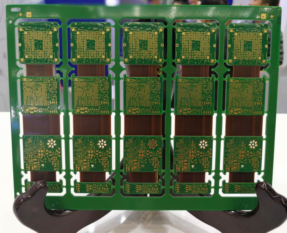
Here is an illustration of a simple rigid-flex PCB:
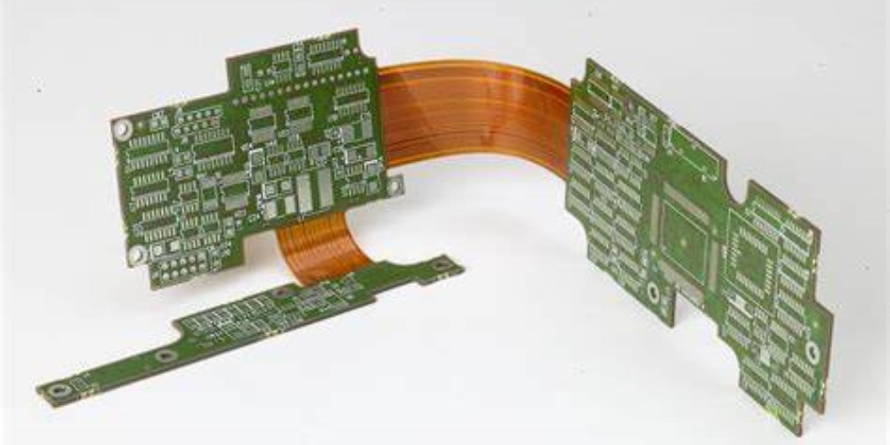
Simple rigid flex PCB
As seen above, the rigid sections provide stability for component mounting while the flexible sections enable dynamic interconnections.
Benefits of Rigid Flex PCBs
Here are some of the key benefits of rigid-flex PCBs:
- Compact design: By folding rigid sections, the circuit can fit into small spaces. This allows for miniaturized and portable designs.
- Flexibility: Dynamic flexing improves reliability in movable parts and high vibration environments. The boards can be bent and twisted repeatedly.
- Layer flexibility: Rigid layers provide stability while thin flex layers enable high density trace routing.
- Weight savings: Eliminates wires and connectors leading to reduced weight. Important in aerospace applications.
- Reliability: Flexible sections absorb stresses and strains improving life cycle. Offers up to 2 million dynamic bend cycles.
- Customizability: Complex 3D shapes are possible increasing freedom of design. Unique form factors can be created.
- Cost savings: Combines multiple PCBAs onto a single board reducing components and assembly cost.
In summary, rigid-flex PCBs enable smaller, lighter and more reliable electronic designs with enhanced flexibility and customizability. The combo of rigid and flex materials provides an optimal combination of stability and interconnectivity.
Design Considerations
Here are some important considerations when designing a rigid-flex PCB:
- Determine the number of rigid layers and flexible layers needed based on circuit complexity and routing density. More layers provide higher trace density.
- Position components on the rigid sections and route traces on the thin flexible layers. Avoid components on flex areas.
- Minimize the number of flex-to-rigid transitions to reduce via complexity. Use stiffeners if needed.
- Manage diferent coefficients of thermal expansion between rigid and flex areas to prevent delamination and cracks.
- Determine optimal board thickness. Rigid sections are typically 0.8 to 1.6mm while flex sections are around 0.1 to 0.2mm.
- Define minimum bend radius for the flex areas based on flex material properties. Polyimide allows tighter folds.
- Clearly specify board outline with rigid and flex sections marked. Indicate locations of cutouts, slots and holes.
- Work closely with your PCB manufacturer during the design process to leverage their design rules and capabilities.
Proper planning of the rigid-flex layout and managing the transitions are critical for reliability.
Manufacturing Process
Rigid-flex PCBs require specialized fabrication processes. Here is a look at the standard manufacturing process flow:
1. Layer Preparation
The individual rigid and flexible layer cores are prepared first. Rigid sections use standard FR-4 material while flex sections use polyimide or other flexible polymer film. Adhesive layers are added to enable lamination between layers.
2. Layer Stackup
The rigid and flex layer cores are stacked up along with bondply layers to achieve the final board thickness. Alignment is critical during layup to ensure trace positions match across layers.
3. Lamination
The layer stackup goes through a high temperature and pressure lamination process. This bonds the layers together into a unified board structure.
4. Drilling
Holes are drilled through the board to create vias for vertical interconnections between layers. Precise laser drilling is required for the small hole sizes.
5. Metallization
The walls of the vias are plated with copper creating a conductive path between layers. Electroless plating and electroplating processes are used.
6. Photolithography
The desired circuit pattern is printed on the layers using photolithographic processes. This transfers the PCB layout onto the copper layers.
7. Etching
The copper is etched away to leave only the desired circuit traces on each layer. The unwanted copper is dissolved using chemical etchants.
8. Solder Mask
A solder mask layer is added to coat the entire board except the solder pads. This provides insulation and prevents solder bridging.
9. Silkscreen
Identifying text and markings are printed on the board using the silkscreen process.
10. Testing
The finished boards are electrically and visually tested. Automated optical inspection checks for defects.
11. Scoring/Routing
The boards are routed to create the final rigid and flex outlines. Flex areas may be scored to allow folding.
12. Assembly
Components are soldered on and connectors mounted to produce the fully assembled PCB ready for use.
Rigid-flex PCB fabrication requires advanced processes, materials, lamination technologies and capabilities. Work with an expert manufacturer to produce a high quality board.
Example Rigid-Flex Applications
Here are some examples of products using rigid-flex PCBs:
Wearable Devices

Rigid flex PCB in a wearable fitness tracker
Wearable products like fitness bands and smart watches benefit from rigid-flex PCBs. The rigid sections provide stability for component mounting while the flex allows the PCB to curve around the wrist or body comfortably. Rigid-flex allows electronics to better conform to the human body.
Laptop Displays
Rigid flex PCB for laptop display (Image source: Semicon)
Laptop displays require flexible connections from the motherboard to the LCD panel. Rigid-flex PCBs meet this need with flex layers routing signals and rigid layers providing stability at component junctions. The dynamic flexing absorbs open/close stresses.
Medical Equipment
Rigid flex PCB enabling healthcare system
Medical devices like patient monitors often have space constraints. Using a rigid-flex PCB allows packing the rigid PCBAs in optimal configurations while the flex sections route between system blocks. This allows for denser, smaller devices.
Consumer Electronics
Rigid flex PCB in a mobile phone (Image source: Altium)
Many consumer devices like mobile phones and gadgets utilize rigid-flex PCBs. Compact folding designs are enabled by having rigid sections for components and dynamic flex layers to interconnect and interface with displays, antennas, batteries etc.
Frequently Asked Questions
Here are some common FAQs about rigid-flex PCBs:
Q: How many layers can rigid-flex PCBs support?
A: Rigid layers are typically limited to 8 layers but flex layers can be added up to 12-16 total layers. More layers increases routing density and complexity.
Q: What are some example rigid/flex materials used?
A: Rigid sections use standard FR-4. Flex materials include polyimide, PEEK, PET, PI/glass etc. Each has different properties.
Q: Can components be assembled on the flex section?
A: It’s recommended to place components only on rigid areas. If needed, only small passives can be mounted on flex areas with adhesives.
Q: What are some failure modes in rigid-flex boards?
A: Delamination between material layers, cracked traces on flex, component pad separation, via fracture, underfill voids, and improper bending.
Q: What are the typical maximum rigid board thicknesses?
A: Standard rigid thickness is 1.6mm but can go up to 3.2mm with thicker cores. Non-standard processes are needed above that.
Q: What are the minimum bend radius limitations?
A: Polyimide flex can do 0.10-0.15mm radius. Liquid crystal polymer flex allows down to 0.025mm radius folds.
Conclusion
In summary, rigid-flex PCBs provide an optimal combination of stability and interconnectivity for compact and reliable electronic designs. The rigid sections offer component mounting stability while the flexible circuits enable dynamic interconnections between subsystems. Rigid-flex opens up space and weight savings through 3D layouts, folding and elimination of wires and connectors. With careful design planning and fabrication, rigid-flex PCBs enable miniaturized and portable electronics to fit into the tight spaces and custom form factors demanded by modern devices.