

What are standard PCB thicknesses?
Printed circuit boards (PCBs) are the backbone of electronics. They provide the foundation on which components are mounted and connected with traces. PCB thickness is an important design consideration impacting mechanical strength, weight, spacing, and manufacturability. This article explores common PCB thickness standards used in different applications.
PCB Basics
PCBs consist of an insulating substrate clad with a thin layer of copper that is etched to form the conductive traces and pads. The substrate material is typically fiberglass reinforced epoxy laminate material FR-4, but other insulating materials like polyimide and ceramic can also be used.
The main PCB thickness measurements are:
- Overall thickness – The total thickness from the top to bottom surface of the finished PCB
- Copper thickness – Thickness of the copper foil layer on the outer surfaces
- Dielectric thickness – Thickness of the insulating FR-4 core
What Determines PCB Thickness?
Several factors influence the choice of PCB thickness:
- Number of layers – More layers allow complex routing but increase thickness
- Component height – Tall components mean thicker PCB for sufficient clearance
- Flexibility requirements – Thinner material allows more flex and bend
- Weight and space constraints – Thinner PCBs reduce weight and take up less space
- Manufacturing capabilities – Thicker PCBs over 1.6mm may require special processes
Common PCB Thickness Standards
Many standards exist for PCB thicknesses used in different types of products and applications.
Single-Sided and Double-Sided PCBs
For simple low component density PCBs, single-sided (1 copper layer) or double-sided (2 copper layers) designs are often used. Some common thicknesses for rigid FR-4 PCBs are:
| PCB Type | Overall Thickness |
|---|---|
| Single-sided | 1.0mm, 1.2mm, 1.6mm |
| Double-sided | 1.2mm, 1.6mm |
| Double-sided with thicker copper | 2.0 mm to 2.4 mm |
Thinner 0.6mm to 0.8mm PCBs are also possible but less common as they are more fragile. The thin dielectric makes routing traces under components more difficult due to reduced spacing.
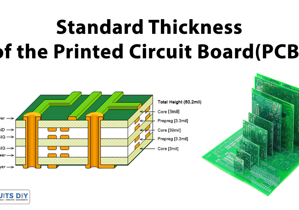
Multi-Layer Boards
For complex, dense PCBs with many components, multiple routing layers allow intricate wiring between pads. Some standard thicknesses for rigid multilayer boards are:
| Number of Layers | Overall Thickness |
|---|---|
| 4-layer | 1.2mm, 1.6mm |
| 6-layer | 1.6mm, 2.0mm |
| 8-layer and above | 2.4mm and up |
High layer counts benefit from thicker dielectrics for easier trace isolation and improved impedance control.
High Frequency and RF Boards
At high frequencies, controlled impedances and layers between the ground planes become critical. Standard thicknesses for radio frequency (RF) PCBs include:
| Type | Overall Thickness |
|---|---|
| RF Boards | 1.6mm |
| High-Speed Digital | 2.4mm to 3.2mm+ |
Added dielectric improves impedance tolerance and reduces cross-talk. Thicker dielectrics also allow more room for multiple ground layers.
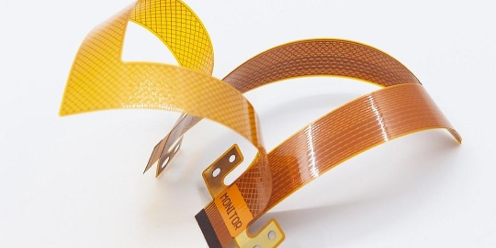
Flexible Circuits
Flexible PCB substrates like polyimide allow bending and flexing. Common flex board thicknesses are:
| Type | Overall Thickness |
|---|---|
| Single-sided flex | 50μm – 130μm |
| Double-sided flex | 75μm – 150μm |
Very thin flexible materials down to 12.5um are also available. Polyester flex film allows more flexibility while polyimide has higher heat resistance.
PCB Copper Thickness Standards
In addition to dielectric thickness, the thickness of the copper foil is also standardized. The table below shows common copper weights used:
| Copper Weight | Foil Thickness |
|---|---|
| 1⁄3 oz | 0.0012” (0.031 mm) |
| 1⁄2 oz | 0.0014” (0.035 mm) |
| 1 oz | 0.0028” (0.071 mm) |
| 2 oz | 0.0056″ (0.14 mm) |
Thicker copper improves current handling capacity and reduces resistive losses but also increases manufacturing costs. High speed designs tend to use thinner foils.
Specialized and Custom Thickness Standards
Beyond standard FR-4 designs, some applications demand specialized dielectric materials or custom thicknesses.
Metal Core Boards
For high power electronics, the PCB substrate contains an internal thick metal layer, usually aluminum or copper. This functions as both a core structural support and also a heatsinking layer to dissipate heat from power devices. Overall thicknesses tend to range from 2mm to 6mm+.
Thermal Clad Boards
Related to MCPCBs, thermal clad boards have thinner overall dielectric layers but attach thick metal baseplate materials as external heatsinks. This also conducts heat away from hot components. Copper thicknesses of 0.020” to 0.125”+ are often used.
Custom Thickness
While standard thicknesses cover most applications, fully custom PCB thickness specifications are possible for unique mechanical, electrical or thermal needs. Tolerances down to ±0.05mm are achievable but increase costs.
Factors in PCB Thickness Selection
Choosing the optimum PCB thickness requires balancing many interdependent structural, electrical, thermal, and manufacturability factors.
Structural Rigidity
Thicker fiberglass epoxy PCB materials provide more structural strength and prevent warping, twisting or other deformations under temperature cycling. This ensures reliability of solder joints and connections. Minimum thicknesses for handling and assembly must also be considered.
As a rule of thumb, a 1.6mm board is sufficiently rigid for most applications. Going below 1mm risks potential handling damage during assembly. Greater than 2.4-3.2mm may present issues with thickness tolerances, drilling quality and plating adhesion.
Electrical Routing Layers
Complex, dense boards with many components and routing constraints require more layers. Additional layers add thickness but enable intricate wiring paths between pads.

High speed digital designs also call for controlled impedance traces. Wider dielectric gaps reduce electrical noise and cross-talk for cleaner signals.
Component Clearances
Adequate vertical space between the board and taller components is necessary to prevent shorts. Thicker boards provide increased clearance. Height restrictions must also be considered depending on enclosure constraints.
Thermal Performance
While thicker Cu layers aid heat dissipation, overall thicker dielectric reduces thermal conductivity and transfers heat less efficiently from components to external cooling surfaces. Thinner cores are better for thermal performance.
This tradeoff requires analysis of the particular power densities and temperature rise requirements. More aggressive cooling schemes can compensate for thicker board materials.
Manufacturing and Fabrication
Standard PCB processes tend to target thicker boards from 0.4mm up to 1.6mm. Over 2.0-2.4mm requires specialized equipment, drilling tools and plating processes which increase costs. Panel and mechanical spacing requirements may also require thinner laminates.
Common PCB Thickness Guidelines
As a general guideline for starting designs, the following PCB thickness standards will cover most applications:
- Low complexity boards – 1.6mm thickness provides good strength while allowing moderate component heights and densities for simple, low layer count designs.
- Medium complexity boards – Target 2.4mm for increased clearances and improved manufacturing yields on higher layer count boards holding many medium height components.
- Advanced boards – Choose 3.2mm+ thicknesses for very complex routing requirements, RF boards with controlled impedances, and extra clearance for tall components and connectors.
Of course, specific clearances, layer counts, electrical, thermal and mechancial requirements for a given product may dictate moving higher or lower than these initial recommendations.
PCB Thickness Selection Process
Determining the optimum PCB thickness is an iterative process based on evaluating the critical design factors.
1. Define Layout Complexity
First assess approximate component quantities, heights and densities to determine electrical routing complexity. This establishes the minimum necessary layer stackup:
- Low-complexity – Single-sided or double-sided
- Medium-complexity – 4-6 layers
- High-complexity – 8+ layers
2. Choose Initial Thickness
Select an initial thickness based on layer count using the general guidelines. This will be refined in subsequent steps.
3. Check Component Clearances
Review clearances between tallest components and enclosure covers or shields with the initial thickness. If inadequate, increase overall thickness.
4. Confirm Manufacturing Requirements
Discuss preliminary thickness choice with the PCB manufacturer. Thicker boards may necessitate special tools or processes. Revise if needed.
5. Thermal Analysis
Simulate board thermal rise and gradients. If temperature exceed component limits, evaluate thicker copper, thermal clad or thicker dielectrics.
6. Final Structural Analysis
Confirm the design has acceptable mechanical rigidity for handling, assembly and resistance to flexure and twisting across operating temperatures.
Careful analysis of all these interacting factors helps finds the Goldilocks PCB thickness – not too thick, not too thin, but just right!
FAQ
Here are some common questions and answers about standard PCB thicknesses:
Q: How thick are professional PCBs in consumer electronics?
The vast majority of cost optimized commercial electronics target 1.6mm thickness. This balances structural rigidity, weight, height restrictions, thermal performance and ease of manufacture. High end consumer devices may use 2.4mm or 3.2mm standard thicknesses.
Q: What is the normal range for flex PCB thickness?
Most flexible circuits use polyimide substrates in the range of 25um to 150um thickness. Above 200um approaches rigid-flex with limited bend capacity. Below 25um increases risks of handling damage without proper lamination or stiffener plates.
Q: Are there thickness standards for specialized materials like Rogers and Ceramics?
For radio frequency boards made of materials from Rogers Corporation or ceramic substrates, overall thickness depends greatly on dielectric constant, conductor skin depths, and impedance tolerances needed. These are custom analyzed based on electrical performance goals rather than standardized.
Q: Can PCB manufacturers supply non-standard thicknesses if required?
Definitely. While standard thicknesses minimize cost due to common tooling and processes, custom thicknesses to meet specialized product goals are possible. Discuss specific needs with fabricators to determine achievable tolerances and lead times.
Q: Is there an optimum PCB thickness to weight ratio?
This depends greatly on complexity and specific requirements. As a starting point, target 1.6mm for low-mid complexity boards and 2.4mm for complex boards to balance functionality, manufacturability and minimal weight. Thermal clad or metal core boards drive thickness and weight higher as power dissipation needs increase.