


Introduction to PCB Design
Printed Circuit Board (PCB) design is a crucial aspect of electronic product development. A well-designed PCB ensures reliable functionality, optimal performance, and cost-effectiveness. In this comprehensive article, we will explore essential tips and tricks to help you master the art of PCB design. Whether you’re a beginner or an experienced designer, these insights will enhance your skills and streamline your design process.
Understanding the Basics of PCB Design
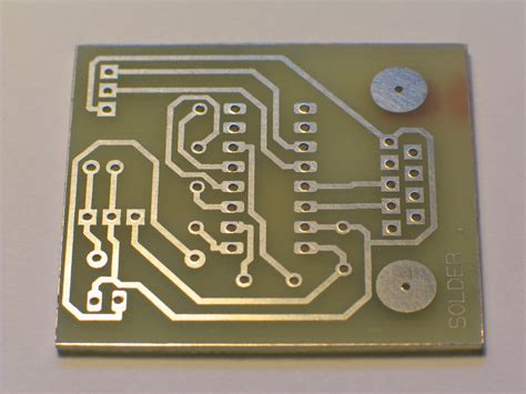
Before diving into advanced techniques, it’s essential to grasp the fundamentals of PCB design. A PCB is a flat board made of insulating material, such as fiberglass or composite, with conductive copper traces etched onto its surface. These traces connect electronic components, forming a complete circuit.
Key Components of a PCB
- Substrate: The insulating base material of the PCB.
- Copper Layers: Conductive layers that carry electrical signals.
- Solder Mask: A protective coating that insulates the copper traces.
- Silkscreen: Text and symbols printed on the PCB for component identification.
- Vias: Conductive holes that connect different layers of the PCB.
PCB Design Software
To create PCB designs efficiently, you’ll need specialized software. Some popular options include:
- Altium Designer
- Eagle CAD
- KiCad
- OrCAD
- Mentor Graphics PADS
These software tools provide a user-friendly interface, extensive component libraries, and powerful design automation features.

Planning Your PCB Design
Before starting your PCB design, thorough planning is essential. Consider the following factors:
Define Your Requirements
Clearly outline the functionality, size constraints, power requirements, and environmental conditions of your PCB. This information will guide your design decisions throughout the process.
Create a Schematic Diagram
Develop a schematic diagram that represents the electrical connections between components. This diagram serves as a blueprint for your PCB Layout.
Choose the Right Components
Select components that meet your design requirements, considering factors such as package size, electrical specifications, and availability. Create a bill of materials (BOM) to keep track of all the components needed.

PCB Layout Techniques
Once you have a solid plan and schematic, it’s time to start laying out your PCB. Follow these techniques to ensure an optimal design:
Component Placement
- Place components logically, minimizing the distance between connected components.
- Consider the flow of signals and power when arranging components.
- Keep sensitive components away from potential sources of interference.
Routing Techniques
- Use the shortest and most direct routes for critical signals.
- Avoid sharp angles and maintain consistent trace widths.
- Provide adequate spacing between traces to minimize crosstalk.
- Use ground planes to improve signal integrity and reduce electromagnetic interference (EMI).
Power and Ground Distribution
- Properly design power and ground planes to ensure stable voltage distribution.
- Use Decoupling Capacitors near power pins to suppress noise.
- Implement star grounding techniques to minimize ground loops.
Thermal Management
- Consider the thermal dissipation requirements of your components.
- Provide sufficient copper area for heat-generating components.
- Use thermal vias to transfer heat from components to other layers or heatsinks.

Signal Integrity and EMC Considerations
Signal integrity and electromagnetic compatibility (EMC) are critical factors in PCB design. Follow these guidelines to ensure reliable performance:
Impedance Matching
- Match the impedance of traces to the source and load impedances.
- Use controlled impedance techniques for high-speed signals.
Crosstalk Reduction
- Provide adequate spacing between sensitive traces.
- Use guard traces or ground planes to isolate signals.
EMI Reduction
- Minimize loop areas to reduce electromagnetic radiation.
- Use shielding techniques, such as grounded enclosures or shielding gaskets.
- Follow proper grounding and filtering practices.
Manufacturing Considerations
To ensure a smooth transition from design to manufacturing, keep these considerations in mind:
Design for Manufacturability (DFM)
- Adhere to the manufacturing capabilities and tolerances of your chosen PCB fabricator.
- Provide clear and accurate documentation, including Gerber files and drill files.
Design for Assembly (DFA)
- Consider the component placement and orientation for easy assembly.
- Provide adequate clearances for automated pick-and-place machines.
- Use standardized component packages whenever possible.
PCB Testing and Validation
- Include test points and probe pads for easy testing and debugging.
- Perform design rule checks (DRC) to identify any layout violations.
- Conduct simulations and prototyping to validate your design before mass production.
Advanced PCB Design Techniques
As you gain experience in PCB design, explore these advanced techniques to take your skills to the next level:
High-Speed PCB Design
- Use controlled impedance techniques for high-speed signals.
- Minimize signal reflections and ringing by proper termination.
- Implement differential signaling for improved noise immunity.
Flex and Rigid-flex PCBs
- Design flexible or rigid-flex PCBs for applications with space constraints or unique form factors.
- Consider the bending characteristics and strain relief techniques for flex PCBs.
PCB Stackup Design
- Optimize your PCB stackup for signal integrity and manufacturability.
- Consider the dielectric constants and thicknesses of the substrate layers.
- Use blind and buried vias for dense designs.
Frequently Asked Questions (FAQ)
- What is the difference between a schematic and a PCB layout?
A schematic represents the electrical connections between components, while a PCB layout shows the physical arrangement of components and traces on the board. - How do I choose the right PCB design software?
Consider factors such as ease of use, feature set, compatibility with your design flow, and cost. Popular options include Altium Designer, Eagle CAD, and KiCad. - What is the importance of Design for Manufacturability (DFM)?
DFM ensures that your PCB design can be efficiently and reliably manufactured. It involves adhering to the manufacturing capabilities and tolerances of your chosen PCB fabricator. - How can I ensure signal integrity in my PCB design?
Signal integrity can be improved by using controlled impedance techniques, minimizing crosstalk, implementing proper grounding and shielding, and following best practices for high-speed design. - What are the benefits of using a ground plane in PCB design?
Ground planes provide a low-impedance return path for signals, reduce electromagnetic interference (EMI), and improve signal integrity by minimizing ground loops and providing shielding.
Conclusion
PCB design is a complex and iterative process that requires a combination of technical knowledge, creativity, and attention to detail. By following the tips and tricks outlined in this article, you can enhance your PCB design skills and create robust, reliable, and high-performance electronic products.
Remember to plan your design carefully, consider manufacturing and assembly requirements, and prioritize signal integrity and EMC. Stay updated with the latest industry trends and technologies to continuously improve your PCB design capabilities.
With practice, patience, and a commitment to excellence, you can master the art of PCB design and bring your electronic ideas to life.
| Topic | Key Considerations |
|---|---|
| Component Placement | – Logical arrangement – Signal and power flow – Interference avoidance |
| Routing Techniques | – Shortest and direct routes – Consistent trace widths – Adequate spacing |
| Power and Ground Distribution | – Stable voltage distribution – Decoupling capacitors – Star grounding |
| Thermal Management | – Sufficient copper area – Thermal vias – Heatsinks |
| Signal Integrity and EMC | – Impedance matching – Crosstalk reduction – EMI reduction |
| Manufacturing Considerations | – Design for Manufacturability (DFM) – Design for Assembly (DFA) – Testing and validation |
| Advanced PCB Design Techniques | – High-speed design – Flex and rigid-flex PCBs – PCB stackup optimization |
Happy PCB designing!