

Introduction to Rigid PCB Boards
A printed circuit board (PCB) forms the backbone of any electronics product. PCBs provide mechanical support and electrical connectivity between electronic components using conductive traces etched from copper sheets and laminated onto a non-conductive substrate.
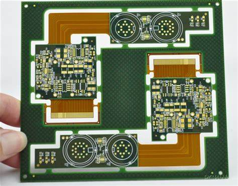
Rigid PCBs employ stiff insulating substrates like FR-4 (glass reinforced epoxy laminate), making themself-supporting. The rigid nature allows rigid PCBs to be designed with minimum board thickness, unlike flex PCBs which require thicker profiles for providing structural stability. This advantage enables efficient utilization of space in electronic products with compact footprints.
In this comprehensive guide, we will explore various aspects of rigid PCB boards, including:
- Benefits of Rigid PCBs
- Rigid PCB Materials
- PCB Layer Stackup
- Rigid PCB Design and Layout
- PCB Manufacturing Process
- Rigid PCB Assembly
- Rigid PCB Applications
- FAQs
Let’s get started!
Benefits of Rigid PCB Boards
Here are some of the major benefits offered by rigid PCB technology:
Structural Rigidity
The rigid laminate material provides excellent mechanical strength to withstand stresses during manufacturing and operation. Minimum board thickness enables compact and lightweight product design.
Ease of Assembly
Component holes and features are dimensionally stable. This allows easy insertion and soldering of components either manually or using automation.
Design Flexibility
Rigid PCBs allow implementation of complex circuit designs with tiny traces and spacing. High component densities can be achieved.
Good Thermal Performance
The dielectric layer offers low thermal resistance allowing heat to dissipate from components attached to the board. This enhances reliability.
Cost-effectiveness
Mature manufacturing processes result in lower costs compared to exotic PCB technologies. Rigid PCBs dominate the consumer electronics segment.
Rigid PCB Materials
Rigid PCB substrates employ insulating dielectric layers reinforced by glass fabric and impregnated with epoxy resin. The commonly used base materials are:
FR-4: This glass-reinforced epoxy laminate offers a good balance of performance and cost for most applications. The temperature rating is 130°C.
High-Tg FR-4: Modified epoxy formulation provides high glass transition temperature (>170°C) for improved thermal performance.
CEM-1: Woven cotton fabric reinforcement results in excellent dimensional stability for multilayer boards.
CEM-3: Glass fabric reinforcement with superior dielectric properties. Used for RF/microwave applications.
PTFE: Polytetrafluoroethylene is used instead of epoxy as the insulating dielectric layer for applications requiring high frequencies and temperatures.
Polyimide: With very high glass transition temperature (>300°C), polyimide finds use in applications involving extreme temperatures such as down-hole drilling.
Other exotic insulating materials are also available for specialized applications.
Popular Core Thicknesses
Rigid PCB core thicknesses are available in imperial and metric sizes:
| Thickness | Common Applications |
|---|---|
| 0.4mm | 2-4 layer consumer electronics |
| 0.6mm | Multilayer boards, improved heat dissipation |
| 0.8mm | Thick multilayer and high current boards |
| 1.0mm | Backplanes, motherboards, and mid-range applications |
| 1.6mm | High layer count multilayer boards |
| 2.0mm | Backplanes, power boards |
PCB Layer Stackup
Layer stackup refers to the sequence of alternating conductive and insulating layers built up to form the final PCB.
A simple 2-layer board will have a core dielectric layer sandwiched between conductive layers on either side. The outer layers are coated with solder mask for insulation and silkscreen for markings.
For a multilayer PCB, multiple conductive layers are separated by thinner prepreg dielectric layers. The sequence is chosen based on electrical connectivity and thermal considerations.
Here are some common rigid PCB layer stackups:
4-Layer Stackup
Prepreg-Core-Prepreg-Conductive-Conductive-Prepreg-Core-Prepreg
Most cost-effective option for complex digital and analog designs. High speed signals can be isolated between layers.
6-Layer Stackup
Prepreg-Conductive-Core-Conductive-Core-Conductive-Prepreg
Provides good isolation between analog and digital sections. Additional routing channels available.
8-Layer Stackup
Prepreg-Conductive-Prepreg-Conductive-Core-Conductive-Prepreg-Conductive-Prepreg
Contains two separate 4-layer sections for extensive routing flexibility. Well suited for advanced electronics.
High layer count PCBs follow similar buildup sequences depending on design complexity and parameters like impedance control.
Rigid PCB Design and Layout
Rigid PCB layout involves placement of components and routing of electrical connections on the board layers. EDA tools allow engineers to design boards and simulate circuit behavior before manufacturing.
Here are some key rigid PCB layout practices:
Component Placement: Parts with electrical connections are grouped into blocks and positioned to minimize track lengths. Heat generating components are placed to facilitate cooling.
Routing: Electrical connections are made with printed copper traces respecting clearance rules. Right angle turns are avoided. Sensitive signals require impedance control.
Stackup Planning: Layer stackup arrangement is optimized based on signal isolation needs and thermal design. Critical nets assigned to inner layers if required.
EMI Control: Noise coupling is minimized by spacing out components generating EMI. Sensitive circuits shielded using ground planes.
Thermal Management: Copper planes and thermal vias help conduct heat away from components. Heatsinks, fans and openings facilitate air flow.
Rigorous simulations are done to verify electrical performance before manufacturing.
PCB Manufacturing Process
Rigid PCB fabrication involves sequentially building up the designed layer structure using lithography to etch the conductive pattern onto each layer.
Major Fabrication Steps
- Inner Layer Processing: Copper foils are laminated onto both sides of the core substrate. Photoresists are coated and imaged to form circuit pattern masks. Etching removes unwanted copper, leaving behind the desired inner layer traces.
- Layer Alignment and Lamination: Align drill holes are created on all layers for later interlayer alignment. The conductive core layers are then assembled in alignment between prepreg dielectric layers and compressed using high temperatures.
- Outer Layer Processing: Similar lithography process used to pattern the outermost circuit layers. Alignment holes ensure layer-to-layer registration.
- Surface Finish Plating: Exposed copper is plated with solder, tin or gold to protect against oxidation and improve solderability.
- Soldermask Lamination: Photoimageable soldermask is applied and patterned to selectively cover board surface, leaving solder pads exposed.
- Silkscreen Printing: Identifying prints and markings are made on soldermask by screen printing.
- Final Finishing: Vias are drilled/plated. Edges chamfered and boards separated by routing. Testing and inspection follows before shipping.
Rigid PCB Assembly
After receiving bare PCBs from fabrication, electronic components are mounted and interconnected to produce finished board assemblies.
Sequence of Assembly Steps
- SMT Placement: Surface mount devices are accurately positioned onto pads on the board using high speed pick and place machines.
- Reflow Soldering: The board passes through a thermal profile in a conveyor oven, allowing the solder paste to reflow and create reliable solder joints.
- Inspection: Assembled boards are visually inspected under microscope and using x-ray imaging to check for defects and quality of component placement/soldering.
- Conformal Coating: Protective coating may be applied selectively over the assembly surface, leaving connectors exposed.
- Through-Hole Soldering: Leaded components are inserted into plated through-holes and hand soldered or wave soldered on the underside.
- Cleaning: Solder flux residues are cleaned using suitable solvents to prevent corrosion.
- Programming: Final firmware/software is loaded onto programmable devices before testing functionality.
- QC Testing: Comprehensive tests conducted to validate assembly performance before shipping.
Rigid PCB Applications
The combination of excellent mechanical rigidity and ease of assembly has made rigid PCBs the substrate of choice for a wide variety of electronics products including:
- Consumer Electronics: Cell phones, tablets, wearables, home appliances.
- Computers and Servers: Motherboards, expansion cards, desktops, laptops.
- Telecom Infrastructure: Networking cards, base stations, optical fiber.
- Automotive: Engine control units, dashboards, infotainment systems.
- Medical Devices: Diagnostic equipment, analyzers, implants.
- Industrial Electronics: Process control systems, robotics, power supplies.
- Military and Aerospace: Avionics, navigation, guidance systems.
- IoT Devices: Sensors, meters, detectors, actuators.
Innovations in materials and fabrication methods have enabled rigid PCBs to keep pace with the rapidly evolving world of electronics over the past decades.
Frequently Asked Questions
Here are some common FAQs related to rigid PCB boards:
Q: What are the key differences between rigid and flex PCBs?
Rigid PCBs use stiff insulating substrates for structural rigidity while flex PCBs use flexible polymer films allowing dynamic flexing during use. Rigid PCBs offer ease of assembly while flex PCBs enable compact mechanisms and moving joints.
Q: How are components attached to a rigid PCB?
Leaded components are inserted into plated through-holes and soldered. SMD components are reflow soldered onto surface pads. Some connectors attach using press-fit pins or fasteners.
Q: What are thermal vias in PCBs?
Thermal vias are holes plated through multiple layers to conduct heat between layers. This allows heat dissipation from inner layers to the board surfaces for cooling.
Q: What is HDI technology in PCBs?
High density interconnect or HDI refers to manufacturing technology allowing ultrafine trace features and high component densities on the board. This meets the needs of miniaturized designs.
Q: What causes failures in rigid PCBs?
Failures can be caused by defects introduced during fabrication or improper assembly. Cracking or delamination can also occur due to thermal cycling during operation.
Summary
Rigid PCB technology enables the efficient and cost-effective translation of electrical circuits into compact and robust physical implementations. Their excellent mechanical and thermal properties have established rigid boards as the workhorse of electronics hardware across consumer and industrial applications. With an in-depth understanding of materials, design practices and manufacturing processes, PCB engineers can continue innovating to meet the needs of a connected world.