

What is PCB Stackup?
PCB stackup refers to the arrangement of layers in a printed circuit board (PCB). It is a critical aspect of PCB design as it determines the board’s electrical properties, mechanical strength, and manufacturability. A well-designed PCB stackup ensures proper signal integrity, minimizes electromagnetic interference (EMI), and reduces manufacturing costs.
Key Components of PCB Stackup
- Core: The base material, typically made of FR-4 (a glass-reinforced epoxy laminate).
- Copper Layers: Conductive layers that carry electrical signals and power.
- Prepreg: Pre-impregnated layers used to bond the core and copper layers together.
- Solder Mask: A protective coating applied to the outer layers to prevent oxidation and short circuits.
- Silkscreen: A layer that contains text and symbols for component placement and identification.
Factors to Consider When Designing PCB Stackup
1. Board Thickness
The thickness of a PCB is determined by the number of layers and the thickness of each layer. Thicker boards are generally more robust and have better thermal dissipation, but they are also more expensive and harder to manufacture. Thinner boards are cheaper and easier to produce but may be less durable and have limited layer counts.
| Board Thickness | Typical Layer Count | Applications |
|---|---|---|
| 0.8mm – 1.6mm | 2 – 4 layers | Simple devices, low-power applications |
| 1.6mm – 2.4mm | 4 – 8 layers | Moderate complexity, mixed-signal designs |
| 2.4mm – 3.2mm | 8 – 12 layers | High-speed digital, complex designs |
| 3.2mm and above | 12+ layers | High-density interconnect (HDI), advanced packaging |
2. Layer Count and Arrangement
The number of layers in a PCB stackup depends on the complexity of the design and the required functionality. A typical 4-layer stackup consists of two signal layers (top and bottom) and two internal planes (power and ground). As the layer count increases, the arrangement of signal, power, and ground layers becomes more critical to maintain signal integrity and reduce EMI.
Common Layer Arrangements
- 4-layer: Signal – Ground – Power – Signal
- 6-layer: Signal – Ground – Signal – Signal – Power – Signal
- 8-layer: Signal – Ground – Signal – Power – Power – Signal – Ground – Signal
3. Material Selection
The choice of materials for the core, prepreg, and copper layers affects the electrical and mechanical properties of the PCB. FR-4 is the most common core material due to its good dielectric properties, thermal stability, and low cost. Other materials, such as Rogers or Isola, may be used for high-frequency or high-speed applications.
Copper thickness is specified in ounces per square foot (oz/ft²). Common copper weights are 0.5 oz/ft², 1 oz/ft², and 2 oz/ft², with thicker copper used for power delivery and high-current applications.
4. Impedance Control
Controlling the characteristic impedance of transmission lines is essential for maintaining signal integrity in high-speed designs. The impedance is determined by the geometry of the trace, the dielectric constant of the surrounding material, and the proximity to reference planes (ground or power).
To achieve consistent impedance, designers must carefully select the trace width, thickness, and spacing, as well as the thickness of the dielectric layers. Specialized tools and calculators are used to determine the optimal geometry for a given stackup and material combination.
5. Via Design
Vias are used to connect traces on different layers of the PCB. The size, type, and placement of vias can significantly impact signal integrity and manufacturability. Some common via types include:
- Through-hole vias: Drilled through the entire board, used for component mounting and layer transitions.
- Blind vias: Connect an outer layer to an inner layer, but do not go through the entire board.
- Buried vias: Connect two or more inner layers, but do not reach the outer layers.
- Microvias: Small-diameter vias (typically less than 0.15mm) used in HDI designs.
When designing vias, consider the drill size, pad size, and anti-pad size (clearance around the via on reference planes) to minimize signal degradation and EMI.

PCB Stackup Design Process
1. Define Requirements
Start by gathering the design requirements, including:
- Board size and shape
- Layer count and arrangement
- Material properties (core, prepreg, copper)
- Impedance targets
- Via types and sizes
- Manufacturing constraints
2. Create Initial Stackup
Based on the requirements, create an initial stackup using a PCB design tool or stackup planning software. Assign layers for signals, power, and ground, and specify the material properties and thicknesses for each layer.
3. Perform Signal Integrity Analysis
Use signal integrity simulation tools to analyze the performance of critical signals in the initial stackup. Check for issues such as impedance mismatch, crosstalk, and EMI. Adjust the stackup and trace geometry as needed to meet the signal integrity targets.
4. Optimize for Manufacturability
Review the stackup with the PCB manufacturer to ensure it can be reliably produced. Consider factors such as:
- Minimum trace width and spacing
- Minimum drill sizes for vias
- Copper balance and symmetry
- Material availability and cost
Make any necessary adjustments to the stackup to improve manufacturability and reduce costs.
5. Finalize and Document
Once the stackup has been optimized for signal integrity and manufacturability, create a final stackup diagram and document the layer assignments, material properties, and any special requirements. Include this information in the PCB design package for fabrication.

Common PCB Stackup Configurations
2-Layer Stackup
A simple 2-layer stackup is suitable for low-complexity designs and consists of a single core with copper on both sides. The top layer is typically used for components and signals, while the bottom layer is used for ground and signals.
| Layer | Material | Thickness |
|---|---|---|
| Top Copper | 1 oz/ft² | 0.035mm |
| FR-4 Core | – | 1.6mm |
| Bottom Copper | 1 oz/ft² | 0.035mm |
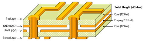
4-Layer Stackup
A 4-layer stackup is a common choice for moderate-complexity designs and provides a good balance between signal integrity and cost. The stackup consists of two signal layers (top and bottom) and two internal planes (power and ground).
| Layer | Material | Thickness |
|---|---|---|
| Top Copper | 1 oz/ft² | 0.035mm |
| FR-4 Prepreg | – | 0.2mm |
| Ground Plane | 1 oz/ft² | 0.035mm |
| FR-4 Core | – | 1.2mm |
| Power Plane | 1 oz/ft² | 0.035mm |
| FR-4 Prepreg | – | 0.2mm |
| Bottom Copper | 1 oz/ft² | 0.035mm |
6-Layer Stackup
A 6-layer stackup is used for more complex designs that require additional signal layers. The stackup typically consists of four signal layers and two internal planes (power and ground).
| Layer | Material | Thickness |
|---|---|---|
| Top Copper | 1 oz/ft² | 0.035mm |
| FR-4 Prepreg | – | 0.2mm |
| Ground Plane | 1 oz/ft² | 0.035mm |
| FR-4 Core | – | 0.6mm |
| Signal Layer 1 | 1 oz/ft² | 0.035mm |
| FR-4 Core | – | 0.6mm |
| Signal Layer 2 | 1 oz/ft² | 0.035mm |
| FR-4 Core | – | 0.6mm |
| Power Plane | 1 oz/ft² | 0.035mm |
| FR-4 Prepreg | – | 0.2mm |
| Bottom Copper | 1 oz/ft² | 0.035mm |

FAQs
1. What is the difference between a core and prepreg in a PCB stackup?
A core is a solid, pre-cured dielectric material that provides the base for the PCB. Prepreg (pre-impregnated) layers are partially cured dielectric materials used to bond the core and copper layers together during the lamination process.
2. How does the dielectric constant of a material affect the PCB stackup?
The dielectric constant (Dk) of a material determines the speed at which signals propagate through the material. Materials with lower Dk values allow for faster signal propagation and are preferred for high-speed designs. The dielectric constant also affects the characteristic impedance of traces, so it must be considered when designing for impedance control.
3. What is the purpose of copper balancing in a PCB stackup?
Copper balancing refers to the practice of ensuring that the amount of copper on each layer of the PCB is roughly equal. This helps to prevent warping and twisting of the board during the manufacturing process, which can cause reliability issues. Copper balancing is achieved by adding copper pours or dummy traces to layers with less copper coverage.
4. How does the PCB stackup affect EMI performance?
The PCB stackup can have a significant impact on electromagnetic interference (EMI) performance. Proper layer arrangement, with dedicated power and ground planes, helps to minimize EMI by providing a low-impedance return path for high-frequency currents. The spacing between layers and the use of shielding techniques, such as ground vias and edge plating, can also help to reduce EMI.
5. What are the benefits of using HDI (high-density interconnect) in a PCB stackup?
HDI technology allows for smaller vias, finer trace widths, and higher layer counts in a PCB stackup. This enables designers to create more compact and complex designs with improved signal integrity and power delivery. HDI also reduces the need for through-hole vias, which can improve manufacturing efficiency and reduce costs. However, HDI designs require more advanced manufacturing processes and may have higher initial setup costs compared to traditional PCB stackups.
Conclusion
Designing an effective PCB stackup is a critical step in the overall PCB design process. By carefully considering factors such as board thickness, layer count and arrangement, material selection, impedance control, and via design, engineers can create stackups that meet the electrical, mechanical, and manufacturing requirements of their projects.
A well-designed PCB stackup ensures proper signal integrity, minimizes EMI, and reduces manufacturing costs. By following the PCB stackup design process and understanding common configurations, such as 2-layer, 4-layer, and 6-layer stackups, designers can create reliable and high-performance PCBs for a wide range of applications.
As PCB technology continues to evolve, with the increasing use of HDI and advanced materials, the importance of effective stackup design will only grow. By staying up-to-date with best practices and collaborating closely with PCB manufacturers, engineers can overcome the challenges of modern PCB design and bring their innovative ideas to life.