


How much does it cost to prototype a PCB?
Introduction
Printed circuit boards (PCBs) serve as the foundation for almost every electronic device, providing the pathways for components to connect and operate. As such, developing a properly functioning PCB is a critical step when designing a new electronic product. However, having a custom PCB professionally manufactured can be expensive, especially for initial prototype boards that will likely require multiple iterations. Understanding the key factors that influence cost is important for budgeting a new device.
This article will analyze the typical pricing structure for PCB prototype services and the common options that impact costs. We’ll examine low volume vs. medium and high volume orders, board size and layers, turnaround time, special requirements, and more. We’ll also look at ways designers can reduce expenses through their design choices. With this information, inventors and engineers can more accurately estimate their PCB prototyping expenses.
Key Factors That Influence PCB Prototype Costs
The costs of professional PCB prototype services are primarily driven by:
Board Quantity
In nearly all cases, per-unit PCB prices decrease significantly as order volumes increase. Smaller quantities incur higher set-up and production costs for manufacturers.
Board Size
The dimensions of a PCB determine the raw materials needed. Larger boards require more substrate and copper materials.
Number of Layers
Multilayer boards with circuits spread across several layers cost more than simple 2-layer boards. Each layer adds expense in materials, lamination, and vias.
Board Complexity
Boards with higher component densities, tighter trace spacing/widths, and smaller holes cost more due to more difficult manufacturing processes.
Lead Time
Rapid turnarounds increase costs due to expedited tooling, supplies, and labor. Standard lead times average 2-3 weeks while “rush” orders add premiums.
Special Requirements
Add-ons like solder masking, silkscreening artwork, gold plating, impedance control, etc. also impact pricing.
We’ll now look at each of these aspects in more detail, including typical price ranges for different options.
PCB Quantities Ordered
One of the foremost factors governing prototype expenses is the number of boards ordered from the manufacturer. Prices are structured in tiers based on quantities, with per-unit discounts kicking in at higher volumes. Let’s examine typical tiers and costs:
Low Volume Prototypes
For initial “proof of concept” testing or design validation where only a handful of boards are needed, almost all PCB manufacturers classify orders for quantities of 10 or less boards as low volume “prototypes”. Sometimes this extends up to 50 boards.
Due to small batch sizes and frequent machine setup/changeovers, these prototype boards come at a premium price, often ranging $50-250 per board or more depending on board specifications. However, they allow testing the basic functionality without high upfront costs during early R&D stages.
Medium Volumes
Once the design is more finalized and additional boards are needed for field testing, debugging, etc., slightly larger quantity orders become necessary. Order sizes of 50-500 boards would fall into the medium volume range. The cost per board drops considerably in this range, down to around $20-100 per board plus smaller added fees.
High Volumes
When moving towards commercial scale production of hundreds, thousands or millions of boards, manufacturers classify these as high volume orders eligible for their lowest pricing tiers. This tier sees dramatic savings from economies of scale, with per-unit costs as low as $2-10 for simple boards. Most manufacturers advertise pricing starting around $100-300 for ~1000 basic boards.
Of course, scaling upwards in volume involves increased risks if any issues emerge requiring physical reworking of many boards or even a full production redo. So levelling up slowly from prototypes to pilot builds allows carefully validating performance before mass production.
Now that we’ve seen typical quantitiy tiers, let’s look at how the physical PCB characteristics also impact pricing.
Board Size
Manufacturing PCBs starts with blank laminated sheets consisting of an insulating substrate with copper layers on one or both sides. The PCB fabrication process then patterns the copper to produce the conductive traces, pads, vias and other features comprising a circuit board.
Larger boards, therefore, require larger starting substrate materials. This contributes directly to material costs. Additionally, bigger boards often necessitate larger equipment for handling, processing, testing and other production steps relative to compact boards. Both factors mean pricing increases with board dimensions.
Most prototype shops have base prices for their smallest board size tier (often around 1-4 in2 / 6-25 cm2). Then pricing progresses upwards in larger size bands based on area. For example, a vendor might charge:
| Board Size | Price |
|---|---|
| < 4 in2 | $100 base |
| up to 20 in2 | + $5/in2 |
| up to 50 in2 | + $4.50/in2 |
| up to 100 in2 | + $4/in2 |
So while a tiny 1” x 1” board might cost $100, a large 10” x 12” board would cost over $580.
Additionally, irregularly shaped boards generally cost more due to material waste when the odd-shaped circuit boards are laid out on the starting substrate sheets during manufacturing panelization.
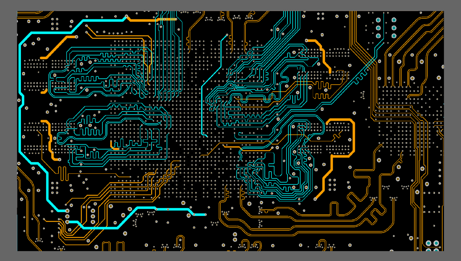
Layer Count
Another major cost contributor is the layer count, dictating the number of copper layers alternating between insulating dielectric. All boards have at least one copper layer on the top and bottom, known as a 2-layer board. This suffices for simpler circuits. When more complex wiring is needed, multilayer boards become essential with additional inner copper layers. Common configs are 4, 6 or 8 layers.
Additional layers multiply the materials, processes and testing time involved in fabrication. Key drivers include:
- Added dielectric substrates and copper foil layers
- Interlayer alignment precision
- Lamination process of gluing layers
- Drilling and plating through-hole vias between layers
- Via fill copper plating
- Increased probability of layer-to-layer shorts
- More complex QA testing
As a ballpark figure, going from 2 to 4 to 6 layers often doubles the pricing at each step. So while an entry-level 2-layer board might cost $100, a similarly sized 6-layer board could run $300-400. The exponential costs of high layer counts make using the fewest necessary layers critical for affordability.
Board Complexity
For a given board size and layer count, further nuances in the design rules and circuit density add onto the base price. Tighter tolerances require upgraded manufacturing capabilities and slower, more precise equipment.
Some key complexity factors include:
Trace/Space Width – thinner traces spaced closer together make for trickier photolithographic imaging and etching. Complex boards with 4/4 mil lines/spaces push fabrication machines to their limits.
Via Tolerance – Smaller microvias save space but require advanced laser drilling vs. standard mechanical drilling. High-density stacked vias also add cost.
Hole Size – Small component holes necessitate thinner drills while large edge plated holes need big equipment. Non-round slots raise difficulty further.
Pad Density – More pads per unit area packing components nearer each other makes fabrication and debugging harder. This depends largely on component choices.
Layer Alignment – Getting traces on separate layers to line up precisely across the layer boundary demands tight process control, especially with many vias.
Special Finishes – Add-ons like immersion gold plating, solder masking and silkscreen printing require additional handling and process steps.
In summary, complexity can vary significantly even for identically sized boards. Simpler boards with 100+ mil line widths and pads cost far less than high density boards pushing 1 mil tolerances with thousands of microvias.
Lead Time
In additional to sheer production costs, turnaround time also plays a major role in pricing tiers. Once customers upload completed Gerber design files, board houses batch jobs for manufacture on the next available production timeline.
Standard lead times for small prototype through medium volume orders range 2-3 weeks on average. This allows efficient batching and workflow. By avoiding rush fees, designers can minimize expenses.
However, accelerating production incurs additional labor, equipment and shipping fees reflected in steeper pricing. Common expedited lead time options include:
- 5-7 day “rush” service at roughly 2-3X standard pricing
- 24-48 hour “emergency” builds at 5X pricing or higher
Therefore, while long lead times might delay development, avoiding unnecessary urgency saves considerable cost especially for iterative prototyping. Careful planning around lead time assumptions prevents getting stuck needing to rush a board redo at the last minute.
Unique Requirements
On top of the core cost contributors above, customized specifications for individual boards introduces further pricing adders. We’ll touch on a few common special requirements:
Controlled Impedance – For high speed signals like PCIe, HDMI, SATA and USB3 ensuring trace impedances involves intensive design rules and validation testing
HDI Technology – Using laser microvias and thin core dielectric enables ultra-high connection density
ENIG Finish – Electroless nickel + immersion gold pads offer excellent solderability/wettability and shelf life
RoHS Compliance – Restriction of Hazardous Substances certification adds materials and process overhead
DFM Checks – Advanced Design for Manufacturability analysis via specialized software maximizes yield
Functional Testing – Applying test patterns and fixture-based electrical validation catches assembly errors
Qualification Testing – Extensive QA test suites (e.g. IPC standards) validate robustness for long-term reliability
The specific needs and risk tolerance on a project determine which specialized options merit the incremental pricing. But foregoing custom elements which won’t actually benefit the product saves unnecessary costs.
Economies of Scale Beyond Prototyping
The pricing dynamics shift once production reaches commercialisation stages seeking longer term scaled supply. Alongside sheer volumes lowering cost, additional methods further reduce expenses:
Panelization – Manufacturing many small PCBs on larger panel “superboards” improves efficiency
Batching – Grouping multiple designs to minimize changeovers cuts overhead
Long Term Agreements – Committing to annual purchase volumes locks in discounted MSA pricing
Alternate Sourcing – Producing in China or other LCC regions cuts direct costs
Continuous Improvement – Design, QA and logistical feedback optimize fabrication and financial performance over product generations
The most successful hardware startups architect flexible supply chains, using prototypes for technical de-risking while planning how to streamline long-run economics for mass production. This powers profitability.
Design Choices Impacting PCB Prototype Pricing
Beyond picking the right PCB manufacturer and service options, designers also play a major role influencing expenses through their architectural choices:
Component Selection – Expensive or obsolete parts that must get sourced via brokers increase BOM costs
Schematic Complexity – Eliminating unnecessary components saves on materials and simplifies assembly and testing
Trace Routing – Using gridded routing architectures matches board houses’ panelization and scoring tooling for better yield and pricing
Standardization – Leveraging consistent footprint families avoids one-off tooling for similar components
Design Margin – Avoiding paper-thin trace spacing tolerances reduces scrap rate by allowing some etch variance
Test Points – Adding spare test points on unused layers provides contingency diagnostic access without consuming key board real estate
Modularity – Enabling subassemblies for incremental PCB portions facilitates faster field upgrades or customization
Design Reviews – Rigorously scrutinizing the design and file outputs prevents avoidable mistakes slipping through to manufacturing
While designers have less flexibility directly controlling manufacturing pricing tiers, they actually have tremendous influence over total prototype expenses when accounting for auxiliary impacts. So focusing both on optimizing the fabrication quoting and whole product development costs gives the full picture.
Example Pricing Breakdown
Let’s walk through a realistic PCB cost estimate given specific design assumptions:
Design Specifications:
- 2 layer board
- 3” x 3” (9 in2)
- 0.5 oz copper
- 10 mil min trace width
- 20 mil min hole size
- 150 mm hole-hole spacing
- HASL lead-free solder finish
- FR4 TG130 substrate
- 1 day DFM check included
- 21 day standard assembly
Order Details:
- Quantity: 5 boards
- No special requirements
- Full turnkey assembly
- Economy shipping to USA
Cost Estimate Breakdown
| Description | Price |
|---|---|
| NRE (tooling set-up fees) | $80 |
| PCB Batch Setup | $125 |
| PCB Cost (5 ct < 10 in2, 2 layer) | $100 |
| PCB Per Unit (5 boards) | $20 |
| Assembly NRE | $50 |
| Assembly Cost (30 comp. per board) | $8 per board |
| Economy Shipping | $35 |
| Total Cost (5 boards) | $565 |
| Per Board Cost | $113 |
So for this fairly straightforward design, small initial prototyping batch and assembly, the total cost works out to $565 for 5 boards, or $113 per board inclusive of everything.
Obviously for different complexity boards and order parameters, the pricing will scale accordingly based on the factors highlighted earlier. But this demonstrates a realistic cost estimate breakdown you might see from an online prototyping service.
This granular analysis helps set expectations upfront and budget for the inevitable design revisions. Now that we’ve explored the key influences on prototype pricing, let’s address some common questions on optimizing fabrication costs.
Frequently Asked Questions
Q: What range of design files do PCB manufacturers accept?
A: The standard inputs are:
- Gerbers – whole PCB image files per layer
- Drill file – NC drill tool instructions
- BOM – component bill of materials
- Pick and place – XY centroid locations
- Netlist – circuit connectivity database
Ensure you export all required files in the correct format to avoid delays or revisions.

Q: Should I use 2 layers or 4 for lowest cost?
A: 2 layers suffice for simple wiring while minimizing expense. But once routing congestion creeps in, shift to 4 layers even if slightly higher cost. The better optimized layout will offset any pricing difference while delivering better quality.
Q: What tolerances work most affordably?
A: For starting points:
- 8mil traces widths
- 8mil trace-to-trace space
- 20mil pad sizes
- 20mil drill holes
- 30mil board edge clearance
Then only shrink further where necessary for compactness rather than arbitrarily mandating ultra-fine features everywhere.
Q: Is it worth paying extra for impedance control or advanced parameters?
A: Only if functionally necessary! For cost sensitive prototypes, omit special capabilities not needed to keep pricing low through initial testing until performance validated.
Q: Should I panelize or batch multiple boards?
A: For prototypes, use whatever format simplifies design validation. But do plan ahead for pilot and production by panelizing and compatibility with final assembly process flow.
Q: Can I reliably mix complexity on multi-project panels?
A: Beware combining widely varying complexity on shared panels. Simpler boards will suffer higher scrap rates. Segregate complex boards into dedicated tighter-tolerance panels.
Conclusion
Prototyping PCBs represents a foundational milestone along the path of conceiving and commercializing an electronic hardware product. While many factors governing prototype expenses remain outside developers direct influence, understanding the key pricing drivers provides helpful visibility when initially budgeting a program.
Additionally, designers do exercise considerable sway over total costs through their specific component choices, board architecture decisions, risk tolerance thresholds and order management. By studying pricing tier structures and strategically guiding technical requirements to strike an optimal balance of capability versus affordability, product teams get the most value from every iteration. This ultimately leads to higher quality commercial solutions with the best business sustainability.