


What is Surface-Mount Technology (SMT)?
Surface-mount technology is a method of manufacturing electronic circuits in which the components are mounted directly onto the surface of a printed circuit board (PCB). This is in contrast to through-hole technology, where the component leads are inserted into holes drilled in the PCB and soldered to pads on the opposite side.
SMT components are typically smaller than their through-hole counterparts, allowing for higher component density and smaller PCB Sizes. This has enabled the development of more compact and portable electronic devices, such as smartphones, tablets, and laptops.
Advantages of SMT over Through-Hole Technology
| Aspect | Surface-Mount Technology | Through-Hole Technology |
|---|---|---|
| Component Size | Smaller, allowing for higher density | Larger, limiting component density |
| PCB Size | Smaller, enabling more compact devices | Larger, requiring more space |
| Manufacturing Speed | Faster, automated process | Slower, often manual process |
| Component Placement | Both sides of the PCB | Typically only one side of the PCB |
| Reliability | Higher, due to stronger solder joints | Lower, due to weaker solder joints |
| Cost | Lower, due to automated process and fewer materials | Higher, due to manual labor and more materials |
History of Surface-Mount Technology
The development of SMT can be traced back to the 1960s, when IBM introduced the first surface-mount package for semiconductors. However, it wasn’t until the 1980s that SMT began to gain widespread adoption in the electronics industry.
Timeline of SMT Development
- 1960s: IBM introduces the first surface-mount package for semiconductors
- 1970s: The development of surface-mount resistors and capacitors begins
- 1980s: SMT gains widespread adoption in the electronics industry
- 1990s: Fine-pitch SMT components become available, enabling even higher component density
- 2000s: Lead-free solder becomes the standard in SMT manufacturing to comply with RoHS regulations
- 2010s: Advanced SMT processes, such as package-on-package (PoP) and system-in-package (SiP), become more prevalent

The SMT Manufacturing Process
The SMT manufacturing process consists of several key steps, each of which plays a critical role in ensuring the quality and reliability of the final product.
Step 1: Solder Paste Application
The first step in the SMT process is the application of solder paste to the PCB. Solder paste is a mixture of tiny solder particles suspended in a flux medium. The paste is applied to the PCB using a stencil and a squeegee, ensuring that the correct amount of paste is deposited on each pad.
Step 2: Component Placement
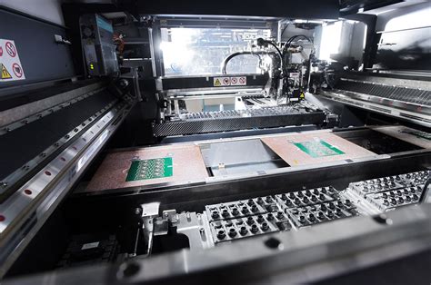
Once the solder paste has been applied, the SMT components are placed onto the PCB using a pick-and-place machine. These machines use computer-controlled nozzles to pick up components from trays or reels and place them onto the PCB with high precision.
Step 3: Reflow Soldering
After the components have been placed, the PCB is sent through a reflow oven. The oven heats the PCB and the components, causing the solder paste to melt and form a strong electrical and mechanical connection between the components and the PCB.
The reflow soldering process typically follows a specific temperature profile, which includes:
- Preheat: The PCB is gradually heated to activate the flux and remove any moisture
- Soak: The temperature is maintained to allow the components and the PCB to reach a uniform temperature
- Reflow: The temperature is increased to melt the solder particles and form the solder joints
- Cooling: The PCB is cooled to allow the solder joints to solidify
Step 4: Inspection and Testing
After the reflow soldering process, the PCB undergoes inspection and testing to ensure that all components are properly soldered and functioning correctly. This may include:
- Visual inspection: Automated optical inspection (AOI) systems or manual inspection to check for visible defects
- X-ray inspection: Used to detect hidden defects, such as voids in the solder joints
- In-circuit testing (ICT): Electrical testing to verify the functionality of individual components and circuits
- Functional testing: Testing the overall functionality of the assembLED PCB
Step 5: Rework and Repair
If any defects are found during the inspection and testing phase, the PCB may need to undergo rework or repair. This may involve removing and replacing defective components, or using specialized tools to repair damaged solder joints.
Step 6: Conformal Coating and Potting
In some cases, the assembled PCB may require additional protection from environmental factors such as moisture, dust, or mechanical stress. This can be achieved through the application of conformal coating or potting.
- Conformal coating: A thin, protective layer applied to the surface of the PCB, covering the components and solder joints
- Potting: Encapsulating the PCB and components in a protective resin or compound

Advanced SMT Processes
As electronic devices continue to become smaller and more complex, advanced SMT processes have been developed to meet the challenges of manufacturing these devices.
Package-on-Package (PoP)
Package-on-package (PoP) is an advanced SMT process that involves stacking multiple Integrated Circuits (ICs) on top of each other to create a single, compact package. This allows for higher component density and reduced PCB size, making it ideal for applications such as smartphones and wearable devices.
System-in-Package (SiP)
System-in-package (SiP) is another advanced SMT process that involves integrating multiple components, such as ICs, passive components, and even micro-electromechanical systems (MEMS), into a single package. This allows for the creation of complete systems in a single, compact package, reducing the overall size and cost of the device.

Frequently Asked Questions (FAQ)
- Q: What are the main advantages of SMT over through-hole technology?
A: The main advantages of SMT include smaller component sizes, smaller PCB sizes, faster manufacturing speeds, the ability to place components on both sides of the PCB, higher reliability, and lower costs. - Q: What is solder paste, and how is it applied to the PCB?
A: Solder paste is a mixture of tiny solder particles suspended in a flux medium. It is applied to the PCB using a stencil and a squeegee, ensuring that the correct amount of paste is deposited on each pad. - Q: What is the purpose of the reflow soldering process?
A: The reflow soldering process is used to melt the solder paste and form a strong electrical and mechanical connection between the SMT components and the PCB. - Q: What types of inspection and testing are performed on assembled PCBs?
A: Assembled PCBs may undergo visual inspection, x-ray inspection, in-circuit testing (ICT), and functional testing to ensure that all components are properly soldered and functioning correctly. - Q: What are package-on-package (PoP) and system-in-package (SiP) processes?
A: Package-on-package (PoP) involves stacking multiple ICs on top of each other to create a single, compact package. System-in-package (SiP) involves integrating multiple components, such as ICs, passive components, and MEMS, into a single package.
Conclusion
Surface-mount technology has revolutionized the electronics manufacturing industry, enabling the production of smaller, more complex, and more reliable electronic devices. By understanding the SMT process and its various steps, from solder paste application to inspection and testing, manufacturers can ensure the quality and reliability of their products. As electronic devices continue to evolve, advanced SMT processes such as package-on-package and system-in-package will play an increasingly important role in meeting the demands of the industry.