


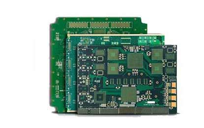
What is a PCB?
A Printed Circuit Board (PCB) is a fundamental component in modern electronics. It is a flat board made of insulating materials, such as fiberglass or plastic, with conductive pathways etched or printed onto its surface. These pathways, known as traces, interconnect various electronic components like resistors, capacitors, integrated circuits (ICs), and connectors, allowing them to function as a complete electronic circuit.
PCBs have revolutionized the electronics industry by providing a reliable, compact, and cost-effective means of assembling electronic devices. They are used in a wide range of applications, from everyday consumer electronics to advanced aerospace and medical equipment.
Advantages of using PCBs
- Compact design: PCBs allow for the miniaturization of electronic devices by efficiently utilizing space and enabling high component density.
- Reliability: The solid connections provided by the etched traces on a PCB ensure reliable electrical connections between components, reducing the risk of short circuits or loose connections.
- Cost-effective: Mass production of PCBs is relatively inexpensive compared to other wiring methods, making them a cost-effective solution for electronic devices.
- Reproducibility: PCBs can be easily reproduced using automated manufacturing processes, ensuring consistency across multiple boards.
- Improved performance: The precise layout and controlled impedance of PCB traces can enhance signal integrity and reduce electromagnetic interference (EMI).
PCB Composition and Structure
A typical PCB consists of several layers, each serving a specific purpose in the overall functioning of the board.
Substrate
The substrate is the foundation of the PCB, providing mechanical support and electrical insulation. Common substrate materials include:
- FR-4: A fiberglass-reinforced epoxy laminate, widely used due to its excellent mechanical and electrical properties, as well as its affordability.
- High-frequency laminates: Materials like Rogers or Teflon are used for high-frequency applications, offering superior dielectric properties and low signal loss.
- Flexible substrates: Polyimide or other flexible materials are used for applications requiring bendable or conformable PCBs.
Copper layers
Conductive copper layers are bonded to the substrate, forming the electrical pathways for the circuit. The number of copper layers can vary depending on the complexity of the design and the required functionality. PCBs can be classified based on the number of copper layers:
- Single-sided PCBs: Copper traces are present on only one side of the substrate.
- Double-sided PCBs: Copper traces are present on both sides of the substrate, with connections between layers made through vias.
- Multi-layer PCBs: These boards have three or more copper layers, with insulating layers separating them. They are used for complex designs requiring high component density and intricate routing.
Solder mask
A solder mask is a thin, protective layer applied over the copper traces, leaving only the exposed areas where components will be soldered. It serves several purposes:
- Insulation: Prevents accidental short circuits by covering the conductive traces.
- Protection: Shields the copper from oxidation and other environmental factors that could degrade its performance.
- Aesthetics: Provides a clean, professional appearance to the PCB, with common colors being green, red, blue, or black.
Silkscreen
The silkscreen layer is a printed overlay on top of the solder mask, used for labeling components, test points, and other important information. It helps with assembly, debugging, and maintenance of the PCB. The silkscreen is typically white, but other colors can be used for improved visibility or aesthetics.

PCB Design Workflow
The PCB design process involves several steps, from concept to final production. Here’s a typical workflow:
- Schematic design: The circuit is designed using a schematic capture tool, defining the components and their interconnections.
- Component placement: The components are arranged on the PCB layout, taking into account factors like signal integrity, heat dissipation, and mechanical constraints.
- Routing: The connections between components are established using copper traces, following design rules and guidelines to ensure proper functionality and manufacturability.
- Design rule check (DRC): The layout is checked against a set of predefined rules to identify and correct any errors or potential issues.
- Gerber file generation: The final PCB design is exported as a set of Gerber files, which are industry-standard formats used for PCB fabrication.
- Fabrication: The PCB manufacturer uses the Gerber files to produce the physical board, including etching, drilling, and applying the solder mask and silkscreen.
- Assembly: The components are soldered onto the PCB, either through manual assembly or automated processes like surface-mount technology (SMT) or through-hole technology (THT).
- Testing and validation: The assembled PCB undergoes various tests to ensure proper functionality, including visual inspection, automated optical inspection (AOI), and electrical testing.

PCB Design Considerations
When designing a PCB, several factors must be taken into account to ensure optimal performance, reliability, and manufacturability.
Signal integrity
Signal integrity refers to the quality of the electrical signals transmitted through the PCB. Factors that can affect signal integrity include:
- Trace width and spacing: Proper trace width and spacing helps maintain consistent impedance and reduces crosstalk between signals.
- Impedance matching: Ensuring that the impedance of the traces matches the impedance of the components and connectors minimizes reflections and signal distortion.
- Grounding and shielding: Adequate grounding and shielding techniques help reduce electromagnetic interference (EMI) and improve signal quality.
Power integrity
Power integrity involves the proper distribution of power to all components on the PCB. Key considerations include:
- Power plane design: Properly designed power planes provide low-impedance power distribution and minimize voltage drop across the board.
- Decoupling capacitors: Placing decoupling capacitors close to power-consuming components helps reduce noise and maintain stable power supply voltages.
- Current-carrying capacity: Ensuring that traces are wide enough to handle the required current helps prevent excessive heating and voltage drop.
Thermal management
Effective thermal management is crucial for maintaining the reliability and longevity of the PCB and its components. Factors to consider include:
- Component placement: Arranging components to evenly distribute heat and minimize thermal hotspots.
- Copper pour: Using copper pour areas to dissipate heat from high-power components.
- Thermal vias: Incorporating thermal vias to transfer heat from components to other layers or heatsinks.
Manufacturing considerations
Designing a PCB with manufacturability in mind helps ensure a smooth and cost-effective production process. Important factors include:
- Design for manufacturing (DFM): Adhering to the manufacturer’s design rules and guidelines for minimum trace widths, spacing, drill sizes, and other parameters.
- Panelization: Arranging multiple PCBs on a single panel to optimize material usage and minimize fabrication costs.
- Testability: Incorporating test points and other features that facilitate automated testing and inspection.

PCB Assembly Techniques
There are two primary methods for assembling components onto a PCB: surface-mount technology (SMT) and through-hole technology (THT).
Surface-mount technology (SMT)
SMT involves placing components directly onto the surface of the PCB and soldering them in place. SMT components have small metal pads or leads that are soldered to corresponding pads on the PCB. Advantages of SMT include:
- Higher component density: SMT components are smaller than THT components, allowing for more compact PCB designs.
- Faster assembly: Automated pick-and-place machines can rapidly place SMT components, enabling high-volume production.
- Better high-frequency performance: SMT components have shorter leads, reducing parasitic inductance and improving high-frequency performance.
Through-hole technology (THT)
THT involves inserting component leads through drilled holes in the PCB and soldering them on the opposite side. THT components are generally larger and more robust than SMT components. Advantages of THT include:
- Mechanical strength: THT components are securely attached to the PCB, providing better mechanical stability and durability.
- Ease of manual assembly: THT components are easier to handle and solder manually, making them suitable for low-volume or prototype production.
- High-power handling: THT components can dissipate more heat due to their larger size and greater contact area with the PCB.
Mixed assembly
Many PCBs use a combination of SMT and THT components to leverage the advantages of both technologies. For example, a board may use SMT for high-density digital components and THT for power-handling or connectors.
PCB Testing and Inspection
To ensure the quality and reliability of the manufactured PCB, various testing and inspection techniques are employed.
Visual inspection
Visual inspection is the first step in assessing the quality of a PCB. This involves examining the board for any obvious defects, such as:
- Solder bridges or shorts
- Incomplete or excessive solder joints
- Damaged or misaligned components
- Incorrect component placement or orientation
Visual inspection can be performed manually or using automated optical inspection (AOI) systems, which use cameras and image processing algorithms to detect defects.
Automated optical inspection (AOI)
AOI systems compare the manufactured PCB to a reference image of a known good board. They can quickly identify a wide range of defects, including:
- Component presence and absence
- Solder joint quality
- Trace and pad alignment
- Solder paste coverage and volume
AOI is particularly useful for high-volume production, as it can inspect boards much faster than manual methods.
In-circuit testing (ICT)
ICT involves using a bed-of-nails fixture to make electrical contact with specific test points on the PCB. This allows for the testing of individual components and circuits, ensuring that they are functioning correctly and within specified tolerances. ICT can detect issues such as:
- Open or short circuits
- Incorrect component values
- Missing or incorrect components
- Faulty solder joints
ICT is an essential step in ensuring the electrical functionality of the PCB before it is integrated into the final product.
Functional testing
Functional testing involves testing the PCB as a complete system, verifying that it performs its intended function within the specified operating conditions. This may include:
- Power-on testing
- Signal integrity testing
- Environmental testing (temperature, humidity, vibration)
- Electromagnetic compatibility (EMC) testing
Functional testing ensures that the PCB meets the requirements of the end application and is ready for integration into the final product.
PCB Manufacturing Process
The PCB manufacturing process involves several steps, from the initial design to the final product. Here’s an overview of the key stages:
- PCB design: The circuit is designed using CAD software, and the PCB layout is created, taking into account design rules and manufacturing constraints.
- Gerber file generation: The PCB design is exported as a set of Gerber files, which contain all the necessary information for manufacturing, including copper layers, solder mask, and silkscreen.
- PCB fabrication: The manufacturer uses the Gerber files to produce the physical board. This involves several sub-processes:
a. Copper cladding: Copper foil is bonded to the substrate material.
b. Patterning: The desired circuit pattern is transferred onto the copper using photoresist and etching techniques.
c. Lamination: For multi-layer boards, the individual layers are aligned and bonded together under heat and pressure.
d. Drilling: Holes are drilled through the board for through-hole components and vias.
e. Plating: The drilled holes are plated with copper to create electrical connections between layers.
f. Solder mask application: The solder mask is applied to protect the copper traces and prevent short circuits.
g. Silkscreen printing: The component labels and other markings are printed onto the solder mask.
h. Surface finish: A protective surface finish, such as HASL (Hot Air Solder Leveling) or ENIG (Electroless Nickel Immersion Gold), is applied to the exposed copper to prevent oxidation and improve solderability. - PCB assembly: The components are placed and soldered onto the PCB using SMT, THT, or a combination of both.
- Testing and inspection: The assembled PCB undergoes various tests and inspections to ensure proper functionality and quality.
- Packaging and shipping: The finished PCBs are packaged and shipped to the customer for integration into the final product.
Types of PCBs
PCBs can be categorized based on various factors, such as the number of layers, substrate material, and special features. Some common types of PCBs include:
- Rigid PCBs: These are the most common type of PCBs, made with a solid, non-flexible substrate like FR-4. They can be single-sided, double-sided, or multi-layer.
- Flexible PCBs: Made with flexible substrate materials like polyimide, these PCBs can bend and conform to various shapes. They are often used in applications where space is limited, or the device requires movement.
- Rigid-Flex PCBs: A combination of rigid and flexible sections, these PCBs offer the benefits of both types. The rigid sections provide structural support and house most components, while the flexible sections allow for connectivity between the rigid sections or to other parts of the device.
- High-frequency PCBs: Designed for high-frequency applications, these PCBs use special substrate materials with low dielectric constants and low loss tangents, such as Rogers or Teflon. They often incorporate advanced design techniques like controlled impedance traces and ground planes to minimize signal loss and distortion.
- High-density interconnect (HDI) PCBs: These PCBs feature fine pitch traces, small vias, and high component density. They are used in applications requiring miniaturization and high performance, such as smartphones, tablets, and wearable devices.
- Metal-Core PCBs: Designed for high-power applications, these PCBs have a metal core (usually aluminum) that acts as a heatsink, efficiently dissipating heat from power-hungry components. They are commonly used in LED lighting, power electronics, and automotive applications.
PCB Design Software
There are numerous PCB design software packages available, ranging from free, open-source tools to high-end commercial solutions. Some popular options include:
- KiCad: A free, Open-source PCB design suite that includes schematic capture, PCB layout, and 3D visualization tools.
- Eagle: A widely-used PCB design software, now owned by Autodesk, offering schematic capture, PCB layout, and autorouting capabilities. It has a free version with limitations and paid versions with advanced features.
- Altium Designer: A high-end, commercial PCB design package with extensive features for schematic capture, PCB layout, signal integrity analysis, and 3D modeling.
- OrCAD: A comprehensive PCB design solution from Cadence, including schematic capture (OrCAD Capture), PCB layout (OrCAD PCB Designer), and simulation tools (PSpice).
- Mentor Graphics PADS: A PCB design platform offering schematic capture, PCB layout, and simulation tools, suitable for small to medium-complexity designs.
When choosing a PCB design software, consider factors such as ease of use, feature set, compatibility with other tools, and cost. Many software packages offer free trials or limited versions, allowing you to explore their capabilities before making a decision.
PCB Industry Standards and Certifications
To ensure the quality, reliability, and consistency of PCBs, various industry standards and certifications have been established. Some key standards include:
- IPC (Association Connecting Electronics Industries) Standards:
- IPC-A-600: Acceptability of Printed Boards
- IPC-A-610: Acceptability of Electronic Assemblies
- IPC-2221: Generic Standard on Printed Board Design
- IPC-2222: Sectional Design Standard for Rigid Organic Printed Boards
- IPC-6012: Qualification and Performance Specification for Rigid Printed Boards
- UL (Underwriters Laboratories) Standards:
- UL 94: Standard for Safety of Flammability of Plastic Materials for Parts in Devices and Appliances
- UL 796: Standard for Safety of Printed-Wiring Boards
- ISO (International Organization for Standardization) Standards:
- ISO 9001: Quality Management Systems
- ISO 14001: Environmental Management Systems
When choosing a PCB manufacturer, it is essential to ensure that they comply with relevant industry standards and hold appropriate certifications. This helps guarantee the quality and reliability of the PCBs they produce.
Frequently Asked Questions (FAQ)
- What is the difference between a single-sided and double-sided PCB?
- A single-sided PCB has copper traces on only one side of the substrate, while a double-sided PCB has copper traces on both sides. Double-sided PCBs offer more design flexibility and higher component density but are more complex to manufacture.
- What is the purpose of vias in a PCB?
- Vias are plated holes that provide electrical connections between different layers of a PCB. They allow signals and power to be routed from one layer to another, enabling more complex routing and higher component density.
- What is the difference between SMT and THT components?
- SMT (Surface-Mount Technology) components are placed directly onto the surface of the PCB and soldered in place, while THT (Through-Hole Technology) components have leads that are inserted through holes in the PCB and soldered on the opposite side. SMT components are smaller and enable higher component density, while THT components offer better mechanical stability and heat dissipation