

Introduction to Hybrid PCBs
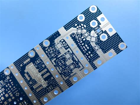
Hybrid printed circuit boards (PCBs) are a type of PCB that combines different substrate materials in a single board. Unlike traditional PCBs that use a single material such as FR-4, hybrid PCBs leverage the unique properties of multiple materials to optimize performance, reliability, and cost for specific applications.
The most common materials used in hybrid PCB construction include:
- FR-4: A low-cost, flame-retardant composite made of woven fiberglass and epoxy resin. FR-4 offers good mechanical strength and electrical insulation properties.
- Polyimide: A high-performance polymer known for its excellent thermal stability, chemical resistance, and flexibility. Polyimide is often used in flexible and Rigid-Flex PCBs.
- Ceramic: An inorganic, non-metallic material with high thermal conductivity, low thermal expansion, and good electrical insulation properties. Ceramics like alumina and aluminum nitride are used in high-power, high-frequency applications.
- Metal Core: A PCB substrate that features a metal base layer, typically aluminum or copper, for enhanced thermal management. Metal core PCBs are used in LED lighting and power electronics.
By combining these materials in a single hybrid PCB, designers can create customized solutions that meet the specific requirements of their application, such as high-speed digital, RF/microwave, power electronics, or harsh environments.
Advantages of Hybrid PCBs
Hybrid PCBs offer several advantages over traditional single-material PCBs:
- Tailored Performance: By selecting the appropriate combination of materials, designers can optimize the PCB’s electrical, thermal, and mechanical properties for specific applications.
- Increased Reliability: Hybrid PCBs can enhance reliability by using materials with better thermal management, lower thermal expansion, and higher chemical resistance in critical areas of the board.
- Space Savings: Combining multiple materials in a single board can reduce the overall PCB Size and thickness, enabling more compact designs.
- Cost Reduction: Hybrid PCBs can lower costs by using expensive, high-performance materials only where necessary and using lower-cost materials elsewhere on the board.

Challenges in Hybrid PCB Design and Manufacturing
Despite their benefits, hybrid PCBs also present unique challenges in design and manufacturing:
Material Compatibility
Ensuring compatibility between different substrate materials is critical in hybrid PCB design. Factors to consider include:
- Thermal Expansion: Mismatched coefficients of thermal expansion (CTE) between materials can lead to stress and delamination during temperature changes.
- Adhesion: Poor adhesion between materials can result in delamination and reduced reliability.
- Electrical Properties: Differences in dielectric constant and loss tangent can affect signal integrity and require careful design considerations.
To address these challenges, designers must carefully select materials with compatible properties and use appropriate bonding techniques, such as adhesives or mechanical fasteners, to ensure reliable inter-layer connections.
Manufacturing Complexity
Hybrid PCBs often require specialized manufacturing processes and equipment, which can increase production complexity and cost. Some key manufacturing challenges include:
- Registration: Aligning and registering different materials during the lamination process can be difficult, especially with thin or flexible substrates.
- Drilling: Drilling through multiple materials with different hardness and thermal properties can cause issues like burrs, smearing, or delamination.
- Plating: Achieving uniform and reliable plating on different materials may require specialized chemical processes or surface treatments.
To overcome these challenges, manufacturers must have experience working with hybrid PCB materials and invest in advanced equipment and process controls to ensure consistent quality.
Design Considerations
Designing hybrid PCBs requires a thorough understanding of the materials’ properties and how they interact with each other. Key design considerations include:
- Material Selection: Choosing the right combination of materials based on the application’s electrical, thermal, and mechanical requirements.
- Layer Stack-up: Defining the appropriate layer stack-up and material thicknesses to optimize performance and manufacturability.
- Thermal Management: Designing efficient thermal paths and using materials with high thermal conductivity in areas that generate significant heat.
- Signal Integrity: Accounting for differences in dielectric properties between materials and designing Controlled Impedance structures to maintain signal integrity.
Designers must also work closely with manufacturers to ensure that their hybrid PCB designs are manufacturable and can be produced reliably and cost-effectively.

Hybrid PCB Material Types
FR-4 and High-Frequency Materials
FR-4 is the most widely used PCB substrate material due to its low cost and good mechanical and electrical properties. However, for high-frequency applications like RF and microwave, FR-4’s high dielectric loss can lead to signal attenuation and degradation.
To address this, hybrid PCBs can combine FR-4 with high-frequency materials like Rogers RO4000 series or Isola I-Tera MT. These materials have a lower dielectric constant and loss tangent, enabling better signal integrity at higher frequencies.
Flexible and Rigid-Flex Materials
Flexible and rigid-flex PCBs use materials like polyimide or liquid crystal polymer (LCP) to create bendable or foldable circuits. These materials offer high flexibility, excellent thermal stability, and good electrical properties.
In hybrid flexible or rigid-flex PCBs, the flexible substrate is typically combined with rigid FR-4 or ceramic materials to create a single board with both flexible and rigid sections. This allows for more complex 3D designs and can reduce the need for connectors between separate rigid and flexible boards.
Ceramic and Metal Core Materials
Ceramic and metal core materials are used in hybrid PCBs for applications that require high thermal conductivity, low thermal expansion, or electrical insulation at high temperatures.
Ceramic substrates like alumina (Al2O3) or aluminum nitride (AlN) offer excellent thermal conductivity, high dielectric strength, and low dielectric loss. They are often used in high-power, high-frequency applications like RF power amplifiers or automotive electronics.
Metal core materials, such as aluminum or copper, provide a high thermal conductivity base layer for efficient heat dissipation. They are commonly used in LED lighting applications or power electronics where thermal management is critical.

Hybrid PCB Material Comparison
The following table compares the key properties of common hybrid PCB materials:
| Material | Dielectric Constant | Dielectric Loss Tangent | Thermal Conductivity (W/mK) | CTE (ppm/°C) |
|---|---|---|---|---|
| FR-4 | 4.3 – 4.7 | 0.02 – 0.03 | 0.3 – 0.4 | 12 – 16 |
| Polyimide | 3.2 – 3.5 | 0.002 – 0.003 | 0.2 – 0.3 | 12 – 16 |
| Rogers RO4350B | 3.48 | 0.0037 | 0.6 – 0.8 | 10 – 12 |
| Alumina (Al2O3) | 9.8 – 10.0 | 0.0001 – 0.0004 | 20 – 30 | 6 – 8 |
| Aluminum Nitride | 8.6 – 8.9 | 0.001 – 0.002 | 140 – 180 | 4 – 5 |
FAQ
- What is a hybrid PCB?
A hybrid PCB is a printed circuit board that combines different substrate materials in a single board to optimize performance, reliability, and cost for specific applications. - What are the most common materials used in hybrid PCBs?
The most common materials used in hybrid PCBs are FR-4, polyimide, ceramic, and metal core substrates. - What are the advantages of using hybrid PCBs?
Hybrid PCBs offer advantages such as tailored performance for specific applications, increased reliability, space savings, and cost reduction by using high-performance materials only where necessary. - What are the main challenges in designing and manufacturing hybrid PCBs?
The main challenges in hybrid PCB design and manufacturing include ensuring material compatibility, dealing with manufacturing complexity, and considering factors like material selection, layer stack-up, thermal management, and signal integrity. - What applications are hybrid PCBs commonly used in?
Hybrid PCBs are commonly used in applications such as high-speed digital, RF/microwave, power electronics, LED lighting, and automotive electronics, where specific electrical, thermal, and mechanical properties are required.
Conclusion
Hybrid PCBs offer a versatile solution for designers looking to optimize their PCBs for specific applications by combining the unique properties of different substrate materials. By understanding the advantages, challenges, and material options available, designers can create innovative and reliable hybrid PCB designs that meet the demanding requirements of modern electronics.
However, the successful implementation of hybrid PCBs requires close collaboration between designers and manufacturers to ensure that the chosen materials are compatible, manufacturable, and cost-effective. As the electronics industry continues to evolve, hybrid PCBs will play an increasingly important role in enabling the next generation of high-performance, reliable, and compact electronic devices.