


What is Double-sided SMT Assembly?
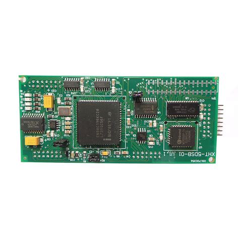
Double-sided Surface Mount Technology (SMT) assembly is a process where electronic components are mounted on both sides of a Printed Circuit Board (PCB). This technique allows for higher component density, improved performance, and reduced board size compared to single-sided SMT or through-hole assembly methods.
Advantages of Double-Sided SMT Assembly
- Increased component density
- Improved electrical performance
- Reduced board size and weight
- Lower production costs
- Faster assembly times
The Double-Sided SMT Assembly Process
The double-sided SMT assembly process involves several steps to ensure the accurate placement and soldering of components on both sides of the PCB.
Step 1: Solder Paste Application
Solder paste, a mixture of tiny solder particles and flux, is applied to the PCB pads using a stencil or screen printing process. The stencil is aligned with the PCB, and the solder paste is spread across the stencil using a squeegee, depositing the paste onto the exposed pads.
Step 2: Component Placement
Surface mount components are placed onto the solder paste-coated pads using pick-and-place machines. These machines use vacuum nozzles or grippers to pick up components from feeders and place them accurately on the PCB. High-speed pick-and-place machines can place thousands of components per hour.
Step 3: Reflow Soldering
After component placement, the PCB goes through a reflow soldering process. The board is passed through a reflow oven, which heats the board to a specific temperature profile. The solder paste melts, forming a permanent electrical and mechanical connection between the components and the PCB pads.
Step 4: Flipping the PCB
Once the first side of the PCB has been assembled and soldered, the board is flipped over to allow for the assembly of the second side. This process requires careful handling to prevent damage to the components already mounted on the first side.
Step 5: Second Side Assembly
The process of solder paste application, component placement, and reflow soldering is repeated for the second side of the PCB. Special attention is given to the alignment of the board and components to ensure proper registration between the two sides.
Step 6: Inspection and Testing
After the double-sided SMT assembly is complete, the PCB undergoes various inspection and testing procedures to ensure the quality and functionality of the assembled board. These may include:
- Automated Optical Inspection (AOI)
- X-ray inspection
- In-Circuit Testing (ICT)
- Functional testing

Challenges in Double-Sided SMT Assembly
While double-sided SMT assembly offers numerous benefits, it also presents some challenges that must be addressed to ensure a successful assembly process.
Component clearance
When designing a PCB for double-sided SMT assembly, it is crucial to consider the clearance between components on opposite sides of the board. Adequate spacing must be maintained to prevent interference and ensure proper soldering.
Thermal Management
During the reflow soldering process for the second side, the components on the first side are exposed to heat again. This can potentially damage heat-sensitive components. To mitigate this risk, designers must carefully select components and design the PCB layout to minimize thermal stress.
Board Warpage
The repeated exposure to high temperatures during the double-sided SMT assembly process can cause the PCB to warp or twist. This can lead to misalignment of components and soldering defects. Using appropriate PCB materials, controlling the reflow temperature profile, and implementing proper board support can help minimize warpage.
Component Tombstoning
Tombstoning is a defect that occurs when a component stands up on one end during the reflow soldering process. This is more likely to happen in double-sided SMT assembly due to the additional heat exposure. Proper pad design, solder paste selection, and reflow profile optimization can help prevent tombstoning.

Best Practices for Successful Double-Sided SMT Assembly
To ensure a successful double-sided SMT assembly process, consider the following best practices:
- Design for Manufacturing (DFM): Collaborate with your PCB manufacturer early in the design process to ensure your board layout is optimized for double-sided SMT assembly.
- Component Selection: Choose components that are compatible with the double-sided SMT assembly process and can withstand the required temperature profiles.
- Stencil Design: Use appropriate stencil thickness and aperture design to ensure proper solder paste deposition on both sides of the PCB.
- Process Control: Implement strict process controls, including temperature profiling, solder paste inspection, and pick-and-place machine calibration, to maintain consistency throughout the assembly process.
- Quality Assurance: Employ comprehensive inspection and testing procedures to identify and correct any defects or issues early in the assembly process.

Frequently Asked Questions (FAQ)
1. Can all components be used in double-sided SMT assembly?
Not all components are suitable for double-sided SMT assembly. Some components, such as certain electrolytic capacitors and connectors, may not withstand the repeated exposure to high temperatures. It is essential to select components that are rated for the double-sided SMT assembly process.
2. How does double-sided SMT assembly affect the cost of PCB production?
While double-sided SMT assembly may require additional equipment and processing steps compared to single-sided assembly, it can ultimately lead to lower production costs. The increased component density and reduced board size enabled by double-sided assembly can result in material savings and more efficient use of production resources.
3. What is the minimum component spacing required for double-sided SMT assembly?
The minimum component spacing for double-sided SMT assembly depends on various factors, such as the component package size, PCB Thickness, and soldering process parameters. As a general guideline, a minimum spacing of 0.5mm to 1mm between components on opposite sides of the board is recommended. However, it is best to consult with your PCB manufacturer for specific design guidelines.
4. Can double-sided SMT assembly be used for high-reliability applications?
Yes, double-sided SMT assembly can be used for high-reliability applications, such as those in the aerospace, medical, and automotive industries. However, it is crucial to follow strict design guidelines, use appropriate components, and implement robust process controls to ensure the reliability and performance of the assembled PCBs.
5. What is the maximum number of layers that can be assembled using double-sided SMT?
The maximum number of layers that can be assembled using double-sided SMT is not limited by the assembly process itself but rather by the capabilities of the PCB manufacturer and the design requirements of the specific application. Double-sided SMT assembly can be used for multi-layer PCBs, with some manufacturers capable of assembling boards with 20 or more layers.
Conclusion
Double-sided SMT assembly is a powerful technique that enables the production of high-density, high-performance PCBs. By mounting components on both sides of the board, designers can achieve increased functionality and reduced board size. However, the double-sided assembly process presents unique challenges that must be addressed through careful design, component selection, and process control. By following best practices and collaborating with experienced PCB manufacturers, engineers can successfully implement double-sided SMT assembly in their projects, realizing the benefits of this advanced manufacturing technology.
| Aspect | Single-Sided SMT Assembly | Double-Sided SMT Assembly |
|---|---|---|
| Component Density | Lower | Higher |
| Board Size | Larger | Smaller |
| Design Complexity | Simpler | More Complex |
| Thermal Management | Less Critical | More Critical |
| Production Cost | Higher | Lower |
| Assembly Time | Longer | Shorter |
| Suitable Applications | Simpler Designs | High-Density, High-Performance Designs |
Table 1: Comparison of Single-Sided and Double-Sided SMT Assembly
By understanding the principles, challenges, and best practices associated with double-sided SMT assembly, engineers can leverage this technology to create innovative, compact, and high-performance electronic devices that meet the ever-increasing demands of today’s market.