

Introduction
Rigid-flex printed circuit boards (PCBs) combine rigid and flexible circuitry into a single integrated assembly. They provide solutions for complex and compact electronic designs where flexible interconnections are needed. 16 layer rigid flex PCBs offer even greater interconnect density and signal routing capabilities.
In this article, we will provide a comprehensive overview of 16 layer rigid flex PCB technology, including:
- What are rigid flex PCBs and how do they work?
- Benefits and applications of 16 layer rigid flex boards
- Rigid flex materials and construction
- Design considerations for 16 layer rigid flex
- Manufacturing processes
- Quality testing
- Cost factors
- Major rigid flex PCB manufacturers
Equipped with this knowledge, you will have a thorough understanding of the capabilities and uses of advanced 16 layer rigid flex printed circuits.
What are Rigid Flex PCBs?
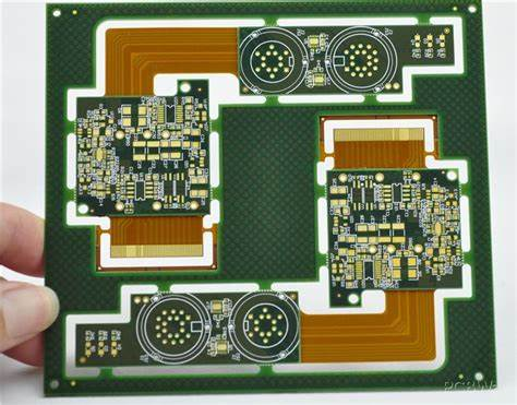
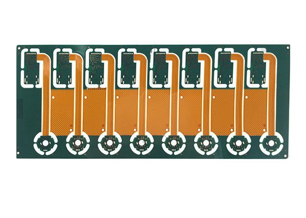
A rigid flex PCB combines rigid PCB substrates and flexible PCB substrates into a single circuit board. The rigid sections provide mechanical support and house complex components and circuitry. The flexible sections enable dynamic flexing interconnections between the rigid areas and components.
Rigid flex PCB with rigid boards connected by flexible circuit sections
This allows the PCB to conform to a variety of form factors and environments, while maintaining high-density integrated circuits across both sections. Common applications include wearable devices, medical equipment, robotics, defense electronics, and aerospace systems.
Rigid flex PCBs can have multiple layers, typically ranging from 2 to 12 or more. 16 layer rigid flex PCBs offer the highest interconnect density, combining 8 or more layers in the rigid sections and 4 or more layers in the flex sections.
Benefits of 16 Layer Rigid Flex PCBs
Here are some of the key benefits that 16 layer rigid flex PCBs provide:
- Extremely dense and complex circuitry integration
- Increased routing channels for high speed signals
- Miniaturization of products and packaging
- Dynamic flexing capacity unmatched by standard PCBs
- Elimination of connectors between PCBs through folded interconnections
- Enhanced reliability with continuous circuits across rigid-flex boundary
- Lighter weight compared to using multiple PCBs
- Reduced system assembly costs
- Accommodation of layer transitions between rigid and flex sections
With up to 700-800 traces per layer, 16 layer rigid flex enables highly advanced compact electronics and miniaturization. The rigid sections provide stability for the thinnest dielectrics and traces. The thin flexible substrates can integrate multilayer flex circuitry into the smallest spaces.
Major Applications of 16 Layer Rigid Flex PCBs
Some of the major applications that benefit from using 16 layer rigid flex PCB technology include:
Aerospace and Defense
- Missiles, radars and weapon systems
- Engine control and monitoring
- Avionics navigational systems
- Spacecraft systems and satellites
Automotive Electronics
- Vehicle control units
- Driver information clusters
- Lane departure warning systems
- Battery and hybrid vehicle circuits
Medical Equipment
- Imaging systems like PET scanners
- Diagnostic devices
- Surgical robots
- Hearing aids
- Wearable patient monitors
Consumer Electronics
- Foldable smartphones
- Tablets and laptops
- Digital cameras
- Virtual reality headsets
- Wearable smart devices
Industrial
- Robotics
- Machine vision systems
- Process control equipment
- Measurement instrumentation
Rigid flex PCBs enable sophisticated electronics to fit into extremely compact form factors that can withstand vibration, shock, and repeated motion. 16 layers are often required to integrate the necessary circuit complexity.
Rigid Flex PCB Materials and Construction
Several types of materials are used in the construction of multilayer rigid flex PCBs:
Rigid Laminates: FR-4, polyimide, FR-5, and metal core are common rigid PCB materials. FR-4 glass epoxy is the most cost effective. Polyimide films like Kapton provide maximum heat resistance.
Flexible Dielectrics: Polyimide is most commonly used but other polymers like PEEK and polyethylene naphthalate (PEN) are options. Polyimide films down to 12 microns provide tight bend radii.
Bonding Films: Acrylic, epoxy, or thermoplastic adhesives bonded in sheets or as inter-layer films. They bond the rigid and flex layers.
Coverlay and Solder Mask: Polyimide, epoxy, silicone rubber, or urethane coats the outer flexible layers. Liquid photoimageable (LPI) solder masks are often used.
Conductors: Copper foils in various weights, with 1/2 to 1 oz being typical for outer layers and 1/3 to 1/2 oz for inner layers. Some flex layers use rolled annealed copper.
Vias: Plated through holes (PTHs) or various types of filled vias connect layers. Blind and buried vias are commonly used.
Construction Process Overview
Multilayer rigid flex PCBs are fabricated through a combination of rigid PCB and flexible PCB processing techniques. Here is a general outline of the multilayer construction process:
- Fabricate individual rigid layer cores and flexible layer cores
- Drill holes for z-axis interconnects on cores
- Metallize drilled holes on cores
- Laminate rigid layer cores together in a press
- Laminate flexible layer cores together
- Bond rigid and flex core sets together using bonding sheets
- Layup any additional flexible layers
- Add outer layer foils
- Image outer layers and plate finishes
- Etch conductors and print solder mask
- Route edges and singulate boards
- Test, inspect, and ship
This is a complex multilayer fabrication process that requires advanced equipment and engineering expertise to manufacture successfully.
Design Considerations for 16 Layer Rigid Flex
Designing a high layer count rigid flex PCB requires paying careful attention to the following parameters:
- Layer stackup sequence
- Layer transitions between rigid and flex sections
- Flex fold areas and dynamic bend radii
- Conductors routing across fold areas
- Clearances for components around folds
- Stiffener locations to manage flex stress
- Z-axis connections between layers
- Matching coefficients of thermal expansion
- Board thickness constraints
- Mitigating via failures through the bend areas
Software tools like CAD, mechanical simulation, and DFM analysis must be used to optimize the design. It is highly recommended to work with an experienced rigid flex PCB manufacturer during the design process to ensure manufacturability.
Manufacturing Process Details
Fabricating a 16 layer rigid flex PCB requires advanced manufacturing techniques and processes:
Imaging: Laser direct imaging (LDI) is used to pattern the finest photolithography features onto layers. Lines/spaces down to 3/3 mil are typical of 16 layer boards.
Registration: Tight layer-to-layer registration on the order of 0.1 mil or less must be held throughout the multilayer lamination process to align high density traces and vias.
Etching: Printed circuit traces are chemically etched down to 1 mil line width on outer layers. Plasma processes are often used.
Drilling: Microvias require laser drilling down to 0.005″ hole size. Mechanical drilling is done for standard vias. Depth control is critical for blind and buried vias.
Metallization: A combination of electroless copper and electrolytic copper are used to plate holes and conductors.
Lamination: Specialized high temperature/pressure lamination presses are used. Z-axis coefficients of thermal expansion are matched. Multiple bonding sheets are often used between specific layers.
Testing: Electrical testing requires finely pitched flying probe testers. Automated optical inspection and x-ray are used.itis critical due to the high cost of scrapped boards.
Quality Testing and Inspection
Rigid flex PCBs require specialized testing to verify the unique aspects of their construction:
- Netlist testing of shorts and opens using flying probe testers
- ICT testing for reliability of z-axis interconnections
- Continuity testing of circuits passing through flexing areas
- Cross sectional analysis of layer alignment
- Automated optical inspection of conductor width, spacing, etc
- Test of chemical resistance of flexible dielectric films
- Adhesion pull strength testing of layer bonding
- Flexibility and dynamic bend cycle testing
- Microsectioning to verify layer stackup, hole fill, etc
- Functional testing of finished populated boards
Each rigid flex PCB manufacturer employs various in-house and third party quality tests to control the reliability and consistency of their complex multilayer processes.
Cost Considerations
In general, rigid flex PCBs have a higher cost compared to conventional rigid PCBs due to:
- Additional processing steps
- More complex fabrication equipment
- Additional bonding and flexible material costs
- Lower yields and higher scrap costs
- Extensive testing and inspection requirements
However, they provide overall system benefits through integration, reduced connectors, smaller form factors, consolidation of assemblies, lower assembly costs, and improved reliability.
For 16 layer rigid flex PCBs specifically, their higher cost is justified for mission-critical electrical systems with:
- Extremely high interconnect density requirements
- Miniaturization needs that cannot be met with fewer layers
- Signal integrity considerations at high frequencies
- Requirements for integration in compact or continuously dynamic bending environments
- Need for elimination of connectors or cables
Major Rigid Flex PCB Manufacturers
Some of the leading global providers of 16 layer rigid flex PCBs include:
| Company | Headquarters |
|---|---|
| TTM Technologies | California, USA |
| Suntak | Hubei, China |
| Flexium | Hsinchu, Taiwan |
| Compass Technology | California, USA |
| Austrian Technologie & Systemtechnik (AT&S) | Austria |
| Guangdong Goworld | Guangdong, China |
| Streamline Circuits | California, USA |
There are also numerous smaller manufacturers around the world who have specialized capabilities in producing advanced multilayer rigid flex circuits.
When selecting a rigid flex PCB supplier, key qualifications to look for include:
- Experience with complex high layer count buildup
- Consistency in quality and attention to detail
- Flex circuit fabrication expertise
- Engineering support for stackup design
- Inventory of various flex dielectric and bonding materials
- Capability to produce fine line traces and spaces
- Sophisticated process controls and inspection systems
- Strong communication and program management skills
Conclusion
16 layer rigid flex PCB technology enables extremely high density integration of circuits in a unique combination of rigid stability and dynamic flexing ability. Rigid flex PCBs are designed to overcome the limitations of standard PCBs through the strategic placement of flexible interconnects between rigid sections.
While rigid flex PCBs require advanced fabrication expertise, they can be a critical enabling technology where reliability, high density, continuous interconnections, and dynamic flexing are key requirements. With over 700 traces per layer, 16 layer rigid flex pushes the boundaries of flex PCB capabilities to their leading edge.
Frequently Asked Questions
Q: What are some key differences when designing a 16 layer rigid flex PCB versus a standard 16 layer rigid PCB?
A: Some key design differences include:
- Fold lines and bend radius requirements
- Transitions between rigid and flexible sections
- Component placement near fold areas
- Routing signals across hinge areas
- Implementing layer transitions
- Minimizing via risks in flexing regions
- Managing mechanical stresses
- Allowing for flex and motion
Q: What are some best practices to ensure reliability of interconnects in 16 layer rigid flex PCBs?
A: Best practices include:
- Utilize stacked or staggered microvias at transitions
- Fill non-plated through holes in flex areas
- Use filled or plugged blind/buried vias
- Implement daisy chain routing for dynamic regions
- Avoid teardrop vias terminating at flex fold lines
- Minimize unsupported span length of traces over hinges
- Implement strain relief features for traces
- Avoid acute angle bends of traces in dynamic areas
Q: How small of a bend radius can a 16 layer rigid flex PCB achieve?
A: With the thinnest polyimide flexible dielectrics, bend radii down to 0.25mm are achievable on the flex layers in a 16 layer stackup. The minimum radius depends on the number of flexible layers used. More flexible layers allow for tighter bend radii.
Q: What are some applications uniquely enabled by the capabilities of 16 layer rigid flex PCBs?
A: Some uniquely enabled applications include:
- Highly compact sensor assemblies
- Wearable health monitoring electronics
- Portable ultrasound devices
- Next generation smartphones
- Advanced vehicular camera systems
- Drone/UAV electronics and controllers
- Missile guidance systems
- Satellite communication modules
Q: What types of file formats are used to manufacture 16 layer rigid flex PCBs?
A: Typical file formats include:
- Gerber files for individual layers
- IPC-2581 for complete designs
- ODB++ provides additional stackup details
- 3D mechanical models
- Configuration drawings to define rigid/flex delineations
- Assembly drawings to guide component placement
CAD tools like Altium, Cadence Allegro, Mentor, Cadence OrCAD, Zuken, and a number of others can export rigid flex PCB designs.