

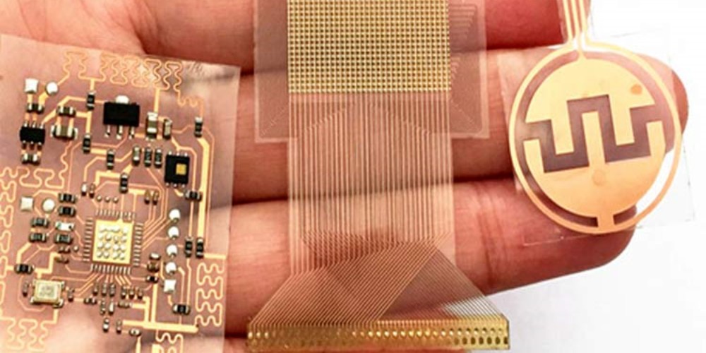
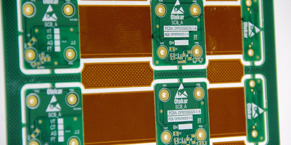
Flexible printed circuit boards (flex PCBs) are made from flexible dielectric materials like polyimide that can bend and flex without damage. Determining the right thickness for your flex PCB design is an important consideration impacting the circuit’s durability, weight, cost, and manufacturability. This guide will examine the key factors to consider when selecting flex PCB thickness.
What is Flex PCB Thickness?
Flex PCB thickness refers to the height of the circuit board from top to bottom. It is typically measured in millimeters (mm) or mils (1 mil = 0.001 inches). The thickness depends on the number and thickness of the conductive, insulating, and protective layers laminated together.
The four main elements contributing to overall flex PCB thickness are:
- Base Material: The flexible dielectric substrate or base material like polyimide film.
- Conductive Layers: The copper foil circuit patterns. This may be a single layer or multilayer.
- Coverlay: A dielectric protective coating over the conductors.
- Stiffener: Optional rigid sections for connecting components.
By understanding the role and options for each layer type, designers can optimize the stackup for their particular flex PCB application.
Typical Flex PCB Thicknesses
Flex PCBs are available in a wide range of thicknesses from 12.5 μm (0.5 mil) up to around 500 μm (20 mils). Some common thicknesses used are:
| Flex PCB Thickness | Description |
|---|---|
| 25-75 μm (1-3 mil) | Ultrathin flex circuits |
| 75-150 μm (3-6 mil) | Thin flex circuits |
| 150-250 μm (6-10 mil) | Medium flex circuits |
| >250 μm (>10mil) | Thick flex circuits |
In general, thinner flex PCBs are more flexible and space saving while thicker flex PCBs are more rigid and durable. The trend has been towards ever thinner flex circuits to reduce size and weight. However, sufficient thickness must remain to meet circuit reliability needs.
Factors that Determine Flex PCB Thickness
Several key factors should be evaluated when selecting an appropriate flex PCB thickness:
Circuit Layer Count
The number of conductive layers (single, double, multilayer) directly impacts thickness. More layers mean greater overall thickness. Two-layer flex circuits with conductors on both sides of the base polyimide are common. 4-6 layer multilayer flex PCBs are also used when more conductors are needed.
Conductor Thickness
Copper foil conductors are typically available in thicknesses from 12.5 μm (0.5 mil) to 70 μm (2.8 mils). Thicker copper provides better current carrying capacity and resilience but increases circuit thickness.
Base Material Thickness
Polyimide film used as the flexible substrate dielectric is available from 12.5 μm (0.5 mil) up to 125 μm (5 mil). Thinner base materials reduce total thickness but may be more prone to damage.
Coverlay Thickness
The coverlay thickness applied over conductors ranges from 25-75 μm (1-3 mils). Thicker coverlay provides greater protection but adds to the total thickness.
Stiffener Thickness
Areas with stiffeners or bondply for component mounting require additional thickness. Stiffeners typically add around 0.1-0.15mm (4-6 mils).
Minimum Bend Radius
A key factor limiting thickness reduction is the minimum bend radius. Thinner flex circuits can accommodate tighter bends. The minimum bend radius may be dictated by application space requirements.
Current Carrying Needs
Thicker copper foils are necessary for higher current. This adds thickness but also allows reducing conductor widths.
Environmental Exposure
More rigidity, conductor thickness, and protective coverlay is required for flex circuits exposed to demanding mechanical, thermal, or chemical conditions.
Pros and Cons of Thinner and Thicker Flex PCBs
Here is a comparison of the advantages and disadvantages of thinner vs. thicker flex PCB designs:
| Thinner Flex Circuits | Thicker Flex Circuits | |
|---|---|---|
| Pros | – Increased flexibility and bendability | – Increased rigidity and durability |
| – Weight reduction | – Withstands higher current loads | |
| – Takes up less space | – Handles harsh environments better | |
| – Allows tighter bend radii | – Easier handling and processing | |
| – Often lower material costs | – Reduces risk of damage | |
| Cons | – Less rugged and prone to damage | – Less flexible, limits bendability |
| – Lower max current capacity | – Heavier and takes up more space | |
| – More challenging handling and assembly | – Often higher material costs | |
| – Higher risk of conductor cracks | – Larger minimum bend radius |
In summary, thinner flex PCBs offer space and weight savings but sacrifice some durability, while thicker flex PCBs are more robust for demanding applications despite drawbacks like higher cost and stiffness.
Typical Base Material Thicknesses
Polyimide films are the most common flexible dielectric substrate used in flex PCBs. Some typical thicknesses for polyimide base materials are:
- 12.5 μm (0.5 mil)
- 25 μm (1 mil)
- 50 μm (2 mil)
- 75 μm (3 mil)
- 100 μm (4 mil)
The thinnest 12.5 μm polyimide films provide maximum flexibility but are also the most fragile. 25-50 μm films offer a good balance of bendability and strength for many flex PCB designs. The thicker 100 μm films approach the rigidity of a rigid PCB while still allowing some flexing.
Other flexible base materials like PEEK or polyethylene terephthalate (PET) are also used in certain applications. These have similar thickness options from 25 μm (1 mil) up to around 125 μm (5 mils).
Typical Coverlay Thicknesses
Coverlay is the protective coating applied over the flex PCB conductor traces. Common coverlay materials include acrylic, polyimide, urethane, and epoxy. Typical coverlay thicknesses are:
- 25 μm (1 mil) – Thin coverlay allows maximum flexibility
- 50 μm (2 mil) – Standard thickness offering good balance of protection and bendability
- 75 μm (3 mil) – Thicker coverlay for highly durable or rigid sections
Examples of Flex PCB Stackups
Here are some examples of common flex PCB layer stackups and overall thicknesses:
2 Layer Flex PCB
- 12.5 μm (0.5 mil) polyimide base
- 17 μm (0.7 mil) copper foil conductors
- 50 μm (2 mil) polyimide coverlay
- Total thickness: 79.5 μm (3.1 mil)
4 Layer Flex PCB
- 25 μm (1 mil) polyimide base
- 2x 17 μm (0.7 mil) copper foil layers
- 25 μm (1 mil) polyimide dielectric bondply
- 50 μm (2 mil) polyimide coverlay
- Total thickness: 134 μm (5.3 mil)
6 Layer Flex PCB
- 50 μm (2 mil) polyimide base
- 3x 35 μm (1.4 mil) copper foil layers
- 2x 25 μm (1 mil) polyimide dielectric bondply
- 75 μm (3 mil) polyimide coverlay
- Total thickness: 290 μm (11.4 mil)
Recommended Minimum Bend Radii for Flex PCBs
The minimum bend radius dictates the smallest radius a flex PCB can be bent without risk of conductor cracks or dielectric damage. Some typical minimum bend radii guidelines:
| Flex PCB Stackup | Minimum Bend Radius |
|---|---|
| 1-2 layer, no coverlay | 0.1 x flex PCB thickness |
| 1-2 layers with coverlay | 0.15 x flex PCB thickness |
| Multilayer, no coverlay | 0.2 x flex PCB thickness |
| Multilayer with coverlay | 0.25 x flex PCB thickness |
So for a 2 layer 79.5 μm flex PCB with coverlay, the minimum bend radius would be around 0.15 x 79.5 μm = 12 mm.
Tighter bend radii increase risks of flex circuit damage. The minimum bend radius limits how narrow a space the flex PCB can fit.
Factors that Allow Thinner Flex PCBs
Advances in materials and manufacturing processes are enabling thinner flex circuits for demanding applications:
- Thinner base films – Polyimide films down to 12.5 μm and below
- Fine line circuits – Finer circuit traces allow reducing copper thickness
- Improved coverlay materials – Thinner coverlay with enhanced protection
- More precision etching – Tight process controls prevent overetching
- Advanced bonding techniques – Thin adhesives enable thinner multilayer flex PCBs
- Smaller component sizes – Chips and passives with smaller pitches and thinner profiles
- Laser micromachining – Allows creating thinner, intricate flex PCB shapes
With innovative designs and advanced manufacturing, flex PCBs of 50 μm (2 mil) total thickness and below can be reliably produced.
Key Takeaways on Flex PCB Thickness
- Flex PCB thickness is determined by conductor, dielectric, coverlay, and stiffener thicknesses
- Typical flex PCB thickness range from 25 μm to 500 μm (1 mil to 20 mils)
- Thinner flex PCBs provide increased flexibility and space savings
- Thicker flex PCBs offer greater durability and current capacity
- Base polyimide thickness, conductor thickness, and number of layers impact overall thickness
- Coverlay and stiffener requirements also affect thickness
- The minimum bend radius often dictates the thinnest usable flex PCB thickness
- Advanced materials and processes allow fabrication of thinner flex circuits
Selecting the optimal flex PCB thickness requires balancing flexibility, durability, space constraints, and manufacturing capabilities for the particular design needs.
Flex PCB Thickness FAQ
Here are answers to some frequently asked questions about determining the right flex PCB thickness:
Q: How thin can flex PCBs be made?
A: The thinnest flex PCBs can be 12.5 μm (0.5 mil) or 25 μm (1 mil) total thickness. However, 12.5 μm is extremely fragile. A 25 μm (1 mil) thickness offers high flexibility with more durability.
Q: What is a typical flex PCB thickness for dynamic or high flex applications?
A: For dynamic flexing applications, a thickness around 50-75 μm (2-3 mils) is common. This maximizes flexibility while still providing good durability and manufacturing yields.
Q: What factors limit how thin flex PCBs can be made?
A: The main constraints are minimum bend radius, conductor current carrying capacity, and susceptibility to damage. Thinner circuits have tighter bend radii but less mechanical robustness.
Q: How do you determine minimum bend radius based on flex PCB thickness?
A: As a guideline, minimum bend radius is around 0.1-0.25 x the total flex PCB thickness, depending on the number of layers. Tighter bend radii increase risk of damage.
Q: Should coverlay thickness be minimized to allow maximum flexing?
A: Not necessarily – coverlay also protects the circuits so reducing it too far impacts reliability. 25-50 μm (1-2 mil) coverlay offers a good compromise for many designs.
Q: Is it always better to use the thinnest flex PCB materials possible?
A: Not always – thinner constructions have higher risks of damage. The thickness should balance flexibility, durability, current loads, and other requirements. Using the thinnest materials that still meets reliability needs is recommended.
Conclusion
Determining the optimal flex PCB thickness requires thorough analysis of the design constraints, circuit layer requirements, minimum bend radius, current loads, and environmental conditions. With an understanding of the tradeoffs between thinner and thicker flex constructions, designers can select a flex PCB stackup that maximizes flexibility and durability for the particular application. Advanced materials and manufacturing processes will continue expanding the possibilities for ever thinner and more robust flex circuits.