

Introduction
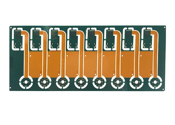
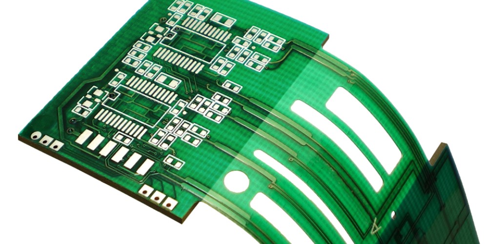
Flex rigid printed circuit boards (PCBs) integrate flexible circuitry with more rigid board substrates to create lightweight and durable electronic interconnect solutions. These hybrid PCBs provide the ability to place circuitry in areas that rigid boards cannot reach, while maintaining stability and protection with rigid board segments.
Flex rigid PCBs offer numerous advantages for electronic product development and are commonly used in aerospace, medical, industrial, automotive, and consumer electronics applications. This article provides an overview of flex rigid PCB technology, manufacturing processes, design considerations, and application examples.
What are Flex Rigid PCBs?
A flex rigid PCB combines flexible circuit materials such as polyimide with traditional rigid fiberglass-reinforced epoxy laminates (FR4) in a single circuit board. The flex circuit portions enable dynamic flexing, twisting, and three-dimensional bending while the rigid sections offer mechanical stability for components and connectors.
Key Features
- Combines flexible and rigid circuitry in one PCB solution
- Flexible portions allow bending, folding, and dynamic movement
- Rigid portions provide structural support and component mounting
- Lightweight and takes up less space than rigid boards alone
- Durable construction withstands vibration, shock, and extreme temperatures
- Allows circuitry placement in unique or tight spaces
- Simplifies assembly and part interconnect compared to cables
Construction
There are three main types of flex rigid PCB construction:
- Rigid-flex: Flexible circuit material bonded to rigid laminate sections
- Flex-rigid-flex: Flexible circuits bonded on both sides of an internal rigid section
- Rigid-flex-rigid: Multiple rigid sections interconnected by flexible circuits
The flexible sections usually consist of a thin polyimide insulator with etched copper traces, while the rigid sections use standard FR4 glass epoxy. Adhesive films bond the materials together into one cohesive circuit board.
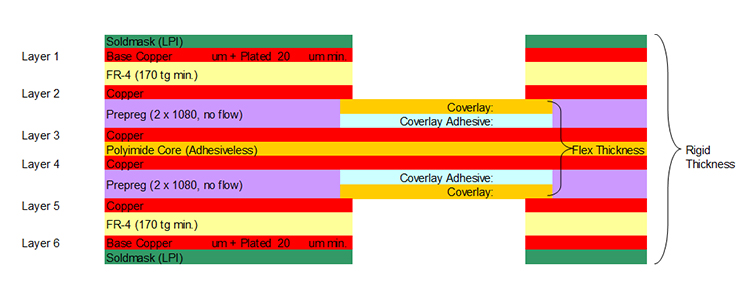
Common flex rigid PCB constructions
Manufacturing Processes
Producing flex rigid PCBs requires specialized fabrication processes to handle both the flexible and rigid materials. Here are some of the key manufacturing steps:
Layer Preparation
The rigid and flexible layers are prepared separately at first. The rigid sections are processed like traditional PCBs with drilling, routing, imaging, and etching to produce the desired conductor pattern.
The flexible layers are laminated with adhesive polyimide films and copper foil. Photolithography forms the circuit traces by masking off the unwanted copper and etching away the exposed metal.
Alignment and Bonding
The individual layers are precisely aligned and bonded together with adhesive films. The adhesive must withstand high temperatures and the different expansion rates of the flexible and rigid materials during processing.
Component Assembly
Standard surface mount technology (SMT) attaches components to the board. The rigid portions often contain most of the components. Flexible areas may have small lightweight components or remain unpopulated.
Via Formation
Laser ablation forms microvias to interconnect the circuitry between layers. This removes material to expose the metal pads for connections. Plated through hole (PTH) vias can also be drilled and plated when connecting rigid board layers.
Final Finishing
Gold plating, hot air solder leveling (HASL), and other finishing processes complete the boards. Test, inspection, and lamination protection ensure the quality of the completed flex rigid PCB assemblies.
Flex Rigid PCB Design Considerations
Designing a successful flex rigid PCB requires paying attention to the interaction between the flexible and rigid sections. Here are some key design guidelines:
- Minimize components in fle areas to reduce stres during flexing
- Plan space for taxicab or island rigid sections for mounting components
- Use wide, rounded traces and tear drop vias in fle areas
- Allow sufficient adhesive overlap of fle and rigid layers
- Accommodate different coefficients of thermal expansion
- Don’t place plated through hole (PTH) vias in fle areas
- Allow room for rigid parts to flex slightly without cracking
- Stress relieve board geometry and distribute flex bend areas
Design considerations for flex rigid PCB layout
Careful planning of the stackup, trace routing, thermal management, and mechanical stress relief are essential to creating durable, high performing flex rigid circuit boards.
Applications and Examples
The unique properties of flex rigid PCBs make them suitable for many products where flexibility, space savings, and durability are desirable. Some common applications include:
Aerospace and Defense
- Aircraft control surfaces and assemblies
- Missiles and weapons systems
- Spacecraft mechanisms and solar arrays
Automotive and Transportation
- Dashboard display and control integration
- Rotating view camera assemblies
- Hinge and joint interconnects
Medical Electronics
- Hearing aids and implants
- Patient monitor connectivity
- Surgical hand tools
Consumer Electronics
- Laptop and mobile device flex interconnect
- Wearable device tight space integration
- Foldable product hinge circuits
Industrial
- Robot articulation and motion control
- Machine tool wiring integration
- Remote sensor connectivity
Flex rigid PCBs continue to see expanded usage as new applications take advantage of their unique rugged and dynamic capabilities. Continued improvements in flexible circuit materials and rigid-flex bonding techniques enable the integration of more layers and higher densities in these hybrid boards.
Flex Rigid PCBs FQA
Here are answers to some frequently asked questions about flex rigid PCBs:
Q: Are flex rigid PCBs more expensive than rigid PCBs?
A: Yes, flex rigid PCBs typically have a higher fabrication cost due to the specialized materials, additional processing steps, lower manufacturing volumes, and more engineering time required. The extra expense may be justified when there are major space, weight, or reliability advantages.
Q: How many times can a flex area be bent before failing?
A: Properly designed flex regions can withstand hundreds of thousands to millions of dynamic bend cycles before wire or base material fatigue occurs. Careful stress relief and strain reduction in layout helps maximize flex life.
Q: Can components be mounted directly on the flexible areas?
A: It is generally advised to keep high mass, tall, or easily damaged components off the thin flexible sections and place them on rigid islands instead. Lightweight SMT chips or bare die can sometimes be mounted directly on polyimide flex circuits.
Q: What are the minimum bend radii for flex circuit traces?
A: Typical flex layer construction supports dynamic bend radii down to 3-5 times the total base copper thickness. For 2 oz copper, around a 0.075″ (1.9mm) radius is the common lower limit.
Q: Can flex rigid PCBs be assembled with automated SMT equipment?
A: Many factories use specialized automation equipment customized for flex PCB transport and assembly. For low volume production, manual assembly may be used if care is taken during handling and clamping.
Conclusion
Flex rigid printed circuit boards provide an optimal blend of flexibility and rigidity for interconnect-intensive electronic products. By combining the unique advantages of both flexible circuits and rigid boards, flex rigid PCBs enable innovative and highly integrated designs across many applications. Continued advancements in materials, fabrication methods, and design tools will drive increased adoption of hybrid flex rigid circuit boards.