


Introduction
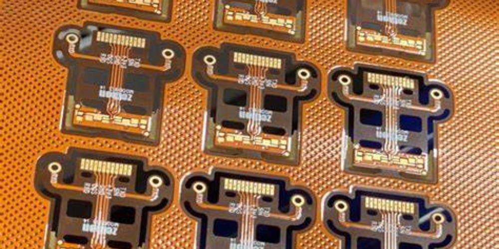
A flexible printed circuit board (flex PCB or flex circuit) is a type of printed circuit board that is thin, bendable and flexible. Unlike rigid PCBs, flex PCBs can be bent, folded or twisted to fit into tight or movable spaces in electronic devices. They are commonly used in consumer electronics, medical devices, aerospace and automotive applications where space is constrained or flexibility is required.
Flex PCBs provide several benefits over rigid PCBs:
- They take up less space and can fit into tight spaces.
- They allow movement and adjustability.
- They improve reliability by reducing the impact of vibrations and mechanical stresses.
- They can be fabricated in smaller quantities at lower costs.
However, flex PCB design also comes with its own set of challenges:
- Careful layout is required to ensure the circuit can flex without damage.
- Special materials, fabrication and assembly processes are needed.
- Electrical performance can be impacted by bending or folding.
- They can be more prone to wear and tear over time.
This comprehensive guide will provide an overview of flex PCB design considerations, best practices, materials, manufacturing and assembly processes.
Flex PCB Design Guidelines
Designing a reliable and functional flex PCB requires attention to the following aspects:
Layer Stackup
The layer stackup defines the number of conductive copper layers separated by flexible dielectric material. Common flex stackups include 1-4 layers, with 1-2 layers being most common. A minimum of 2 layers is recommended for better circuit integrity and reduced noise.
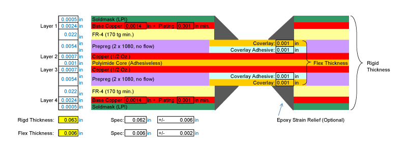
Flex PCB layer stackup example
Conductor Spacing and Width
- Trace spacing on flex PCBs should be at least 6-8 mil (0.15-0.2mm) to avoid shorting.
- Minimum trace width should be ≥ 5 mil (0.127mm) for high yield.
- Wider traces ≥ 8 mil (0.2mm) improve reliability.
- Space around pads and vias should be ≥ 5 mil.
Bend Radius
- Avoid sharp corners. All corners should be rounded with bend radius ≥ 3X conductor thickness.
- Minimum inside bend radius should be ≥ 10X dielectric thickness.
- Tight folds under 3mm require special handling.
Component Placement
- Avoid placing components in areas that will bend or fold repeatedly.
- Use flexible components rated for flexing. Avoid brittle components.
- Distribute components evenly to balance stresses.
- Adhesives must withstand flexing and extremes of temperature.
Stiffening and Support
- Add stiffeners on flex areas with high component density.
- Use covers, shields or carriers for protection in high-stress areas.
Vias
- Unsupported annular rings around vias can crack. Use adhesive or filled vias.
- Minimum annular ring width should be ≥ 5 mil (0.127mm)
- Minimum via diameter should be ≥ 6 mil (0.15mm)
By following these guidelines, flex PCBs can be designed to withstand bending cycles and mechanical stress while maintaining circuit integrity.
Flex PCB Materials
Choosing the right materials is key to designing durable and reliable flex PCBs:
Conductors
- Flex PCB conductors are typically rolled annealed copper foils, with thickness of 1⁄2 oz (18um) or 1 oz (35um) being common.
- Some applications use thicker copper up to 3 oz (105um) for high current capacity.
- Aluminum conductors are occasionally used for reduced cost.
Dielectrics
Common dielectric materials include:
- Polyimide (Kapton): Most commonly used flexible dielectric due to its excellent electrical properties and cut-through resistance. High maximum operating temperature up to 400°C.
- Polyester (Mylar): Lower cost but has poorer chemical resistance than Kapton. Used in less demanding applications.
- Fluoropolymers (PTFE): Provides wide operating temperature range and inertness to chemicals/solvents. Difficult to process.
- Adhesives: Bond flex layers. Acrylic and epoxy are commonly used.
Covercoats
- Covercoat masks help protect conductors from damage.
- Liquid photoimageable (LPI) solder masks are commonly used.
- Conformal coatings and encapsulants can also be applied.
Stiffeners
- Areas with high component density often require stiffeners to avoid flex cracking.
- Common materials include polyimide, PTFE, FR-4, aluminum and stainless steel.
Flex PCB Fabrication
Flex PCBs require specialized fabrication processes:
Imaging
Photolithographic patterning of conductors is typically done by:
- Liquid Photoimageable Solder Mask: More accurate than dry film and provides higher resolution around 6 mil (0.15mm).
- Dry Film Photoresist: Faster and lower cost, resolution around 8 mil (0.2mm).
Etching
Etching of conductors is done using cupric chloride or ammonium persulfate chemical etchants.
Layer Alignment
Aligning layers during lamination requires precision equipment to hold tight tolerances. Common registration options:
- Punched Holes: Holes punched in each layer are aligned over pins. Low cost but +/- 0.3mm tolerance.
- Optical Registration: Uses camera system to optically align layers within +/- 0.05mm tolerance. Higher accuracy but slower.
Via Forming
- Mechanical Punching: Uses dies to physically punch vias through dielectric layers. Higher density but potential for cracked traces.
- Laser Ablation: Uses lasers to selectively ablate and vaporize material to form vias. Very accurate but slower.
Bonding
- Layers are bonded using heat and pressure. Temperature and force are precisely controlled in the lamination press.
- Adhesive sheets or liquid adhesive are used between layers.
- Multiple bonding cycles may be needed to build up multilayer boards.
Finishing
Common finishing steps include:
- Solder mask application
- Legend printing
- Vias plating
- Final trimming/singulation
- Electrical testing
Flex PCB Assembly
Assembly of components requires some unique processes:
Soldering
- Reflow soldering is most common, using SAC (Sn/Ag/Cu) solders.
- Careful profiling of temperature ramps is needed to avoid damage.
- Wave soldering can also be used but can cause more thermal stress.
Component Attachment
- Flexible adhesives are used to attach SMT components. Common choices:
- Silicone adhesives
- Acrylic adhesives
- Urethane adhesives
- Anisotropic conductive films (ACF) can also attach some components.
Rework
- Manual soldering with fine tip irons is preferred over hot air tools.
- Preheating is important to avoid excessive thermal gradient.
Cleaning
- Aqueous cleaners must be used instead of harsh solvents.
- Ultrasonic cleaning risks damage to traces.
Conformal Coating
- Coatings protect against environmental exposure.
- Silicones, acrylics, urethanes and parylene can be used.
- Select flex-compatible products.
With proper materials and processes, high quality and reliable flex PCB assemblies can be manufactured.
Applications of Flex PCBs
Some common applications that benefit from using flexible PCBs include:
Consumer Electronics
Flex PCBs are ubiquitous in consumer devices like mobile phones, tablets, laptops and wearables that require compact, moveable interconnects between components. Common examples include:
- Display interconnects and flip-chip bonding
- Flexible antennas and sensors
- Hinged or sliding mechanisms e.g. phone/laptop hinges
- Interconnections between PCBs e.g. main board to camera module
Medical Devices
Healthcare applications like patient monitoring systems, hearing aids and medical implants utilize flex circuits to provide connections that undergo repeated bending with body movement. Flex PCBs enable:
- Wearable health sensors
- Intravenous catheters and surgical tools
- Endoscopes and probes
- Pacemakers and prosthetic devices
Automotive
Vehicles make extensive use of flex PCBs in applications like:
- Seat heaters
- Overhead console wiring
- Door mechanisms and mirrors
- TPMS tire pressure sensors
- Hybrid/EV motor sensors and control
Aerospace and Military
Space constrained aerospace and military devices operate in high vibration environments often turning to flex PCBs for:
- Avionics systems
- Missile guidance systems
- Unmanned aerial vehicles
- Soldier-worn electronics
Industrial
Industrial equipment benefiting from flex PCBs includes:
- Robotics and machine tools
- POS credit card readers
- HVAC and appliance controls
- IoT and IIoT sensors
As electronics become more compact and require greater mechanical compliance, flexible PCB technology enables innovative solutions across industries.
Flex PCB Design Tools
To assist engineers with flex PCB design and layout, several PCB design software platforms provide dedicated flex and rigid-flex design capabilities:
- Altium Designer – Provides specialized flex design rules, dynamic clearance checking, stackup visualization and 2D/3D folding modeling.
- Cadence Allegro – Features constraint manager for electrical and mechanical rules, automatic fold lines and bundled lengths for measurement.
- Mentor Xpedition – Integrated rigid-flex design environment with length tuning, 2D folding analysis and adaptive layout.
- Zuken CR-8000 – Extensive flex/rigid-flex design tools including cross-section editor, 2D/3D bending simulations and mechanical analytics.
Utilizing these advanced PCB design software platforms helps engineers design flex and rigid-flex circuits for optimal manufacturability and reliability.
Flex PCB Design: Frequently Asked Questions
Q: What are some typical applications for flex PCBs?
A: Common applications are consumer electronics (phones, laptops, displays), medical devices (sensors, hearing aids, implants), automotive (sensors, door mechanisms), aerospace (avionics, UAVs) and industrial electronics (robotics, POS systems). Essentially any space constrained device needing dynamic mechanical performance.
Q: What are recommended minimum trace widths and spacings?
A: Minimum trace width is around 5 mil (0.127mm), while 8 mil (0.2mm) or greater improves reliability. Trace spacing should be at least 6-8 mil (0.15-0.2mm) as a baseline. Spacing around pads and vias should be 5 mil or greater.
Q: Should traces be routed on one layer or both sides?
A: For mechanical reliability, it is generally preferred to route signals on one side only and use the other side as a ground plane. This helps minimize cracking from asymmetric forces during flexing. High density designs may require routing on both sides.
Q: How many layers are typical for most flex PCBs?
A: Simple flex circuits usually only require 1-2 metal layers. As complexity increases, 2-4 layers becomes more common for improved impedance control and shielding. Beyond 4-6 layers, the flex PCB will be difficult to bend and fold repeatedly.
Q: What test and inspection methods are used to ensure flex PCB quality?
A: Electrical testing validates continuity and functionality. Automated optical inspection looks for defects and workmanship flaws. IST testing checks layer misregistration. Cross-sectioning inspects plated through holes. Ultrasonic and x-ray inspection also help detect subtle flaws in the flex PCB.
Conclusion
Flex PCB technology enables innovative and compact product designs across a wide range of industries. However, flex PCB layout requires careful planning for the dynamic mechanical rigors and stresses. Following design guidelines and leveraging the right materials and processes ensures robust and reliable flex circuits. As electronics trend towards smaller, lighter and more complex, flex PCBs will continue seeing expanded adoption thanks to their versatility and durability.