


Can PCB be flexible?
Introduction to flexible PCBs
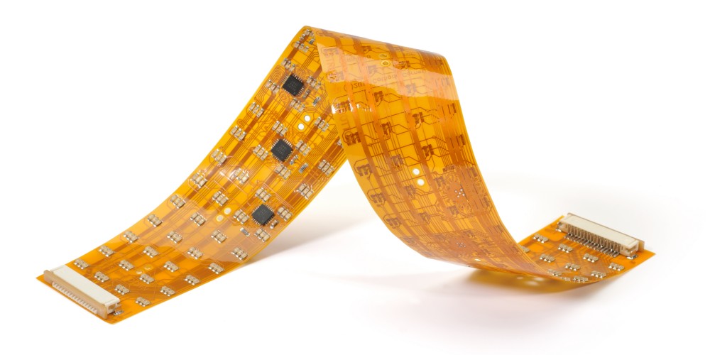
A printed circuit board (PCB) is a board that connects electronic components using conductive tracks and pads. Traditional PCBs use rigid insulating boards made of materials like FR-4. However, advances in materials and manufacturing processes have enabled the development of flexible PCBs (FPCBs).
An FPCB uses a thin insulating flexible base material that allows the PCB to bend and flex. This allows them to be integrated into products with irregular or dynamic shapes. FPCBs are extremely useful when space is limited or when the circuit needs to flex and move. Some common flexible PCB applications include:
- Wearable devices
- Medical devices
- Consumer electronics
- Internet of Things (IoT)
- Automotive electronics
Benefits of flexible PCBs
Flexible PCBs offer several advantages over their rigid counterparts:
Dynamic adaptability: The flexible board can bend, twist, and fold to accommodate movable or irregularly-shaped applications. This dynamic adaptability allows flexible circuits to fit into spaces too small or complex for rigid boards.
Lightweight and thin: FPCBs use extremely thin flexible base materials, reducing weight and allowing layer stacking for increased density. An FPCB can be 90% lighter than a similar FR-4 board.
Enhanced reliability: The base material absorbs shock/vibration instead of transmitting it to solder joints like a rigid board. This dampening ability improves reliability and product lifetimes.
Design freedom: FPCBs allow for more creative industrial design features like custom curved enclosures and wearable or skin-safe products.
Cost savings: FPCB’s small size can reduce materials costs. And improved reliability results in lower servicing/replacement costs over rigid PCBs.
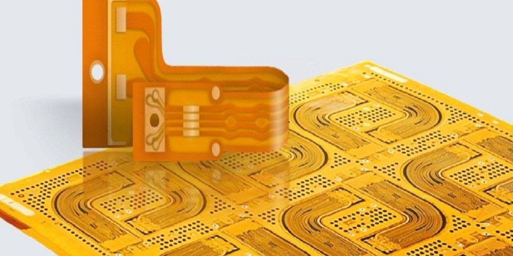
Construction of a flexible PCB
While traditional PCB fabrication methods can be used, FPCBs require some specialized design considerations, materials, and manufacturing processes to create a functional flexible board.
Materials
The core structural component of an FPCB is the flexible dielectric base material. While rigid FR-4 composites are too brittle, common flexible base materials include:
- Polyimide (PI): PI offers excellent thermal stability and chemical resistance. It’s a popular high-performance FPCB material, but is more expensive than PET.
- Polyethylene terephthalate (PET): PET provides electrical insulation along with good chemical/thermal resistance properties. It’s generally cheaper than PI but has lower maximum operating temperatures.
- Polyphenylene sulfide (PPS): With extremely high heat deflection temperatures, PPS maintains mechanical stability in high-temperature environments that would melt other polymers.
- Fluoropolymers (PTFE): PTFE offers robust chemical inertness paired with useful high-frequency electrical properties. However, PTFE boards are relatively rigid with poor tear strength.
The conducting layers are typically made of rolled annealed copper foil around 18μm to 70μm thick. Etching defines the conductive tracks and pads. Specialized flexible coverlay or solder mask layers can provide insulation or limit solder spreading.
Fabrication techniques
Because FPCB materials are thinner and more delicate than rigid boards, specialized fabrication processes have been developed, including:
Laser direct imaging (LDI): Laser lithography patterns resist layers to replace traditional etching processes. This helps avoid damage from chemical processing.
Layer alignment fiducials: Alignment marks help mitigate layer misalignment over large flexible boards.
Advanced plating processes: Electrolytic and electroless nickel/gold techniques provide oxidation resistance while allowing solderability.
Meticulous handling: Humidity/contamination control and specialized FPCB handling equipment reduce defects and yield loss over large delicate flex board panels.
Typical flexible PCB stackup
While designs vary across applications, most flex circuit layer stacks incorporate some common elements:
| Layer | Typical Thickness | Description |
|-|-|-|
| Base Material | 25μm – 130μm | Flexible dielectric support structure |
| Rolled Copper Foil | 18μm – 70μm | Conductive circuit traces and pads |
| Coverlay/Mask | 25μm – 75μm | Solder/insulation masking over traces |
| Adhesive | 25μm – 50μm | Bonds coverlay and assists flexibility |
| Stiffener (optional) | 100μm – 400μm | Layer to locally rigidize flex board sections |
Advanced FPCBs may also utilize specialized outer coatings for environmental protection. Common options include conformal coatings for moisture/contamination resistance or metal-clad layers for electromagnetic interference (EMI) shielding.
Flexible PCB design considerations
Designing a functional FPCB requires specialized considerations across electrical, mechanical, and manufacturing domains:
Electrical design
Controlled impedance: Careful trace dimensioning helps tune circuit impedance for high-speed signals. This avoids impedance discontinuities and reflections.
Layer stacking: Multiple thin copper and adhesive layers enable high component density and complex routing. Sections with many layers may require vias or holes connecting layers.
EMI mitigation: Features like ground planes or metal shielding layers help control electromagnetic interference.
Mechanical design
Avoiding mechanical failures requires analyzing flex stresses and material limits:
- Minimum bend radius: Trace routing should avoid requiring overly tight folds exceeding material yield points and fracture limits.
- Dynamic flex cycle analysis: Simulate folding cycles and develop testing procedures that mimic product movement without inducing early fatigue or cracking failure.
- Reinforcement: Components or flex areas prone to wear may need extra adhesive or clad stiffener layers.
Manufacturing design
Panel utilization: Careful layout maximizes board quantity per panel while considering handling stresses.
Tooling holes: Registration holes outside circuitry areas assist precise laser imaging and depanelization.
Support elements: Unrouted connects hold boards in place during production to improve handling and quality.
Applications and examples
Modern flexible circuits power a huge array of products. Some top modern application categories include:
Wearable and medical devices

- Implanted devices
- Pacemakers
- Hearing aids
- Fitness bands
Consumer electronics and IoT

- Smartwatches and wristbands
- Smartphones
- Virtual reality
- Wearable technologies
Automotive and aerospace

- Automotive sensors
- Heads-up displays
- Seat occupancy detectors
- Vehicle control modules
- UAV/drone circuits
With applications requiring compact, lightweight, dynamic circuits, flexible PCB usage across sectors is consistently growing around 6% per year. As technology advances, engineers continue finding innovative solutions with flex boards.
Common flexible PCB myths
Despite the rise of flex PCBs, some common misconceptions still exist around their capabilities and manufacturing.
Myth 1: Flexible PCBs are only for simple circuits
Reality: Modern flexible boards utilize advanced materials and buildup processes to produce complex multilayer circuits nearly as intricate as rigid boards. High layer counts with thousands of components are achievable.
Myth 2: Flexible PCBs cannot handle significant power

Reality: While traces widths and current limits differ from rigid boards, certain flex materials like polyimide allow substantial power handling. Clever power plane integration and load balancing can enable ≥10A circuits.
Myth 3: FPCB production cannot scale effectively
Reality: Improved fabrication tools tailored for thin flexible materials can maintain yields over large 18”x24” panels. And unlike rigid boards, flex PCBs allow nesting irregular board shapes to maximize panel space.
Myth 4: Flex PCBs cannot withstand harsh environments
Reality: Certain materials offer impressive environmental resistance. For example, PTFE-based flex cores maintain function across -100°C to 260°C temperatures and in many chemical environments.
Flexible PCB limitations
However, flexible PCBs have some inherent limitations to consider before selecting for an application:
Fine pitch constraints: The flexible material’s coefficient of thermal expansion complicates high-density component placement. Practical connection pitch is typically > 0.15mm.
Lower current limits: Narrower traces intrinsically handle lower amperages than thick rigid board traces. Power planes help spread current when higher power is unavoidable.
Cost: Specialized base film materials, fabrication equipment, lower panel utilization factors, and greater scrap losses increase cost relative to rigid PCB solutions.
Longer lead times: Flexible PCB production involves specialized tools and processes. And whole panel processing steps mean small defects scrap an entire panel. Together, these currently extend lead times up to 4-6 weeks.
The future of flexible PCB technology
Engineers continually pioneer new techniques to improve flexible printed circuit boards. On the horizon, expect advances in materials, design tools, fabrication methods and end-user products:
- New conductive and base materials will enable higher frequency, higher reliability solutions.
- Improved modeling and analysis will facilitate dynamic mechanical simulation with more accurate predictions.
- Additive manufacturing and printed electronics aim to increase efficiency and design complexity.
- Growth in medical diagnostics, wearables, and consumer goods will drive broader flexible PCB adoption.
Conclusion
With the drive toward smaller, lighter, and more powerful electrical systems across industries, flexible PCBs provide invaluable adaptability and space savings compared to conventional rigid boards. Careful design consideration around electrical, mechanical, and manufacturing demands allows modern flex circuits to deliver robust and reliable interconnect solutions. While limitations still exist, continual innovation promises exciting expansions in flex PCB capabilities.
Flexible PCB Frequently Asked Questions
What is the typical minimum bend radius for a flexible PCB?
The minimum bend radius varies across different flexible PCB materials, stackups, and construction methods. But for standard polyimide and PET cores, typical minimum inside bend radii range from 2 to 10 times the total board thickness depending on factors like layer count, conductor type, and flex tension. Dynamic folding applications require larger minimum radii.
Can components be mounted directly on flexible PCBs?
Yes, components can be either soldered directly onto FPCB conductive pads or attached using conductive or anisotropic adhesive films. The thin, delicate nature of flex circuits does impose component size and footprint limitations compared to rigid PCBs. But compatibility continues improving with specialized packaging.
Why would stiffeners be used on an otherwise flexible PCB?
While most flex board advantages come from global physical compliance and bending, localized stiffeners help mitigate damage in designated high-stress areas. Common locations include approaching sharp through-hole edges, bordering heavy components prone to fall-off, shielding sensitive RF circuitry, and guarding connectors from peel failures during mating cycles.
How many flexing cycles can a typical FPCB withstand?
A robust flexible PCB design validates reliability across thousands to millions of dynamic flexing cycles depending on the flex radius, materials used, and application stresses. Precision modeling based on IPC-2223A or IPC-6013D test standards helps qualify cycle lifetime through accelerated test data extrapolation and estimation methodologies.
How are components attached to flexible circuits?
Common flex PCB component attachment methods include conductive adhesive bonding, solder attachment, socketing, direct gold wire bonding, and mechanical fastening. The chosen approach balances production factors like process temperatures/tolerances with application demands like shock/vibration resilience and repair/rework needs.