


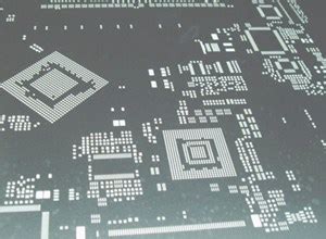
Introduction to PCB Stencils
PCB stencils are thin metal sheets with cutouts that allow solder paste to be precisely applied to printed circuit boards (PCBs) during the assembly process. They are an essential tool in modern electronics manufacturing, enabling the efficient and accurate placement of surface mount components on PCBs.
Benefits of Using PCB Stencils
- Improved solder paste application accuracy
- Increased production speed and efficiency
- Consistent solder joint quality
- Reduced solder paste waste
- Compatibility with a wide range of component sizes and types
Types of PCB Stencils
There are several types of PCB stencils available, each with its own advantages and applications.
Laser-Cut Stencils
Laser-cut stencils are created using high-precision laser cutting machines. They offer several benefits:
- High accuracy and repeatability
- Quick turnaround times
- Suitable for complex designs and fine pitch components
- Durable and long-lasting
Electroformed Stencils
Electroformed stencils are made using an electroplating process, resulting in a highly precise and uniform surface. They are ideal for:
- Ultra-fine pitch components
- High-density PCB designs
- Applications requiring exceptional solder paste release
- Long production runs
Nano-Coated Stencils
Nano-coated stencils feature a special coating that improves solder paste release and prevents solder paste from sticking to the stencil. They offer:
- Improved solder paste release
- Reduced stencil cleaning frequency
- Extended stencil life
- Consistent print quality over time

Stencil Design Considerations
To ensure optimal performance, several factors must be considered when designing PCB stencils.
Aperture Size and Shape
The size and shape of the stencil apertures directly impact the volume and distribution of solder paste applied to the PCB. Some key considerations include:
- Aperture width and length
- Aperture wall angle
- Aperture aspect ratio
- Rounded or square aperture corners
Stencil Thickness
Stencil thickness plays a crucial role in determining the amount of solder paste deposited on the PCB. Factors to consider when selecting stencil thickness include:
- Component pitch and size
- Solder paste type and viscosity
- PCB Surface Finish
- Desired solder joint profile
Stencil Material
The choice of stencil material depends on several factors, such as:
- Durability and wear resistance
- Compatibility with cleaning processes
- Cost and availability
- Laser cutting or electroforming suitability
Common stencil materials include stainless steel, nickel, and polyimide.

Stencil Printing Process Optimization
To achieve the best results with PCB stencils, it is essential to optimize the stencil printing process.
Printing Parameters
Key printing parameters to consider include:
- Squeegee pressure and speed
- Separation speed
- Print stroke length
- Stencil snap-off distance
Proper adjustment of these parameters ensures consistent solder paste deposition and minimizes print defects.
Stencil Alignment
Accurate stencil alignment is critical for achieving precise solder paste placement on the PCB. There are several methods for ensuring proper alignment:
- Fiducial recognition using machine vision systems
- Pin-in-paste alignment for through-hole components
- Manual alignment using alignment marks or guides
Solder Paste Selection
Selecting the appropriate solder paste for your application is crucial for achieving the desired print quality and solder joint reliability. Some factors to consider include:
- Solder paste alloy composition
- Powder particle size and shape
- Flux type and activity level
- Viscosity and rheological properties
| Solder Paste Type | Alloy | Particle Size | Flux Type | Viscosity |
|---|---|---|---|---|
| No-Clean | SAC305 | Type 3 | ROL0 | Medium |
| Water-Soluble | SnPb | Type 4 | ORM1 | Low |
| RoHS-Compliant | SN100C | Type 5 | REL0 | High |

Stencil Maintenance and Cleaning
Proper maintenance and cleaning of PCB stencils are essential for ensuring consistent print quality and extending stencil life.
Cleaning Methods
Regular cleaning of stencils removes solder paste residue and prevents aperture clogging. Common cleaning methods include:
- Manual cleaning with solvents and wipes
- Automated stencil cleaning systems
- Ultrasonic cleaning for thorough residue removal
Inspection and Storage
Periodic inspection of stencils helps identify wear, damage, or contamination that may affect print quality. Proper storage of stencils between uses is also important:
- Store stencils in a clean, dry environment
- Use protective covers or containers to prevent damage
- Avoid exposure to extreme temperatures or humidity
Advanced PCB Stencil Services
As the complexity of PCB designs continues to increase, there is a growing demand for advanced PCB stencil services.
Custom Stencil Design
Many stencil manufacturers offer custom stencil design services to meet specific customer requirements. These services may include:
- Aperture size and shape optimization
- Stencil thickness recommendation
- Design review and modification
- Prototype stencil fabrication
Stepped Stencils
Stepped stencils are designed with multiple thickness levels to accommodate components of varying heights on a single PCB. They offer several advantages:
- Improved solder paste Volume Control
- Reduced risk of component tombstoning
- Better solder joint reliability for mixed-height components
Embedded Stencils
Embedded stencils are permanently attached to the PCB, eliminating the need for a separate stencil during the assembly process. They are particularly useful for:
- High-volume production runs
- PCBs with very fine pitch components
- Applications requiring precise solder paste deposition
3D Printed Stencils
3D printed stencils are an emerging technology that offers unique advantages over traditional stencil manufacturing methods. They enable:
- Rapid prototyping and iteration
- Complex stencil geometries and features
- Localized stencil thickness control
- Cost-effective low-volume production
Choosing a PCB Stencil Supplier
Selecting the right PCB stencil supplier is crucial for ensuring the quality and reliability of your PCB Assembly process.
Experience and Expertise
Look for a supplier with extensive experience in stencil manufacturing and a deep understanding of the PCB assembly process. They should be able to provide expert advice and guidance on stencil design and selection.
Manufacturing Capabilities
Ensure that the supplier has the necessary manufacturing capabilities to meet your specific requirements, such as:
- Laser cutting or electroforming
- Nano-coating or other specialized finishes
- Quick turnaround times
- Prototyping and low-volume production
Quality Control and Certifications
A reputable PCB stencil supplier should have robust quality control processes in place and hold relevant industry certifications, such as:
- ISO 9001 for quality management systems
- ISO 14001 for environmental management systems
- IPC standards for stencil design and fabrication
Customer Support and Service
Choose a supplier that offers excellent customer support and service, including:
- Responsive communication and technical support
- Flexible ordering and delivery options
- Competitive pricing and lead times
- Comprehensive documentation and tracking
Frequently Asked Questions (FAQ) about PCB Stencils
- Q: What is the difference between laser-cut and electroformed stencils?
A: Laser-cut stencils are created using high-precision laser cutting machines, while electroformed stencils are made using an electroplating process. Laser-cut stencils are suitable for most applications, while electroformed stencils are ideal for ultra-fine pitch components and high-density PCB designs. - Q: How do I choose the right stencil thickness for my PCB?
A: The choice of stencil thickness depends on factors such as component pitch and size, solder paste type and viscosity, PCB surface finish, and the desired solder joint profile. Generally, thinner stencils are used for finer pitch components, while thicker stencils are used for larger components and higher solder paste volumes. - Q: What is the purpose of nano-coating on PCB stencils?
A: Nano-coating is a special surface treatment applied to PCB stencils that improves solder paste release and prevents solder paste from sticking to the stencil. This results in improved print quality, reduced stencil cleaning frequency, and extended stencil life. - Q: How often should I clean my PCB stencils?
A: The frequency of stencil cleaning depends on factors such as the type of solder paste used, the print volume, and the environmental conditions. As a general rule, stencils should be cleaned every 4-8 hours of continuous printing or whenever print quality begins to deteriorate. - Q: Can 3D printed stencils replace traditional laser-cut or electroformed stencils?
A: While 3D printed stencils offer unique advantages such as rapid prototyping, complex geometries, and localized thickness control, they are not yet a complete replacement for traditional stencil manufacturing methods. 3D printed stencils are best suited for low-volume production and prototyping, while laser-cut and electroformed stencils remain the preferred choice for high-volume production and demanding applications.
Conclusion
PCB stencils are a critical component of the modern PCB assembly process, enabling the precise and efficient application of solder paste to PCBs. By understanding the types of stencils available, design considerations, process optimization techniques, and maintenance requirements, you can ensure the highest quality and reliability of your PCB assembly.
When selecting a PCB stencil supplier, look for a company with extensive experience, advanced manufacturing capabilities, robust quality control processes, and excellent customer support. By partnering with the right supplier and implementing best practices for stencil design and use, you can achieve optimal results and stay ahead of the curve in today’s fast-paced electronics industry.