

What is PCB Impedance matching?
PCB impedance matching is a technique used in printed circuit board (PCB) design to ensure that the impedance of the transmission lines on the board matches the impedance of the components and devices connected to them. This is important because impedance mismatches can cause signal reflections, which can lead to signal integrity issues, such as signal distortion, ringing, and crosstalk.
Impedance matching is particularly important in high-speed digital circuits, where the rise and fall times of the signals are very short. In these cases, even small impedance mismatches can cause significant signal integrity problems.
Types of Impedance Matching
There are two main types of impedance matching:
- Source Termination: In this method, a resistor is placed in series with the source (driver) to match the impedance of the transmission line. This method is simple and effective, but it can reduce the signal amplitude and increase power consumption.
- Parallel Termination: In this method, a resistor is placed in parallel with the load (receiver) to match the impedance of the transmission line. This method does not reduce the signal amplitude, but it can increase power consumption and may require additional components.
PCB Design Considerations for Impedance Matching
When designing a PCB for impedance matching, there are several factors to consider:
Transmission Line Geometry
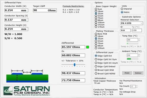
The geometry of the transmission lines on the PCB can have a significant impact on their impedance. The width, thickness, and spacing of the traces, as well as the dielectric constant and thickness of the PCB substrate, all contribute to the characteristic impedance of the transmission lines.
To achieve a specific characteristic impedance, the geometry of the transmission lines must be carefully designed. This can be done using specialized PCB design software that includes impedance calculation tools.
Material Selection
The choice of PCB substrate material can also affect the impedance of the transmission lines. Different materials have different dielectric constants, which can impact the characteristic impedance of the traces.
Common PCB Substrate Materials include:
- FR-4: A glass-reinforced epoxy laminate that is widely used in PCB fabrication. It has a dielectric constant of approximately 4.5.
- Rogers: A family of high-performance PCB substrate materials that offer low dielectric loss and stable dielectric constants over a wide frequency range. They are commonly used in RF and microwave applications.
- Polyimide: A high-temperature, flexible PCB substrate material that offers excellent electrical and mechanical properties. It has a dielectric constant of approximately 3.5.
Stackup Design
The PCB Stackup design can also impact the impedance of the transmission lines. The number and arrangement of the copper layers, as well as the thickness and material of the dielectric layers, can all affect the characteristic impedance of the traces.
A common stackup design for impedance-controlled PCBs is the microstrip configuration, where the signal traces are routed on the top or bottom layer of the board, and a solid ground plane is placed on the adjacent layer. This configuration provides a well-defined reference plane for the signals and helps to control the impedance of the traces.
Via Design
Vias are used to connect traces on different layers of the PCB, but they can also introduce impedance discontinuities if not designed properly. To minimize the impact of vias on impedance, they should be placed strategically and sized appropriately.
One approach to via design is to use blind or buried vias, which are vias that do not extend through the entire thickness of the board. This can help to reduce the length of the via stub, which can minimize the impact on impedance.
Another approach is to use via stitching, where multiple vias are placed in close proximity to each other to create a low-impedance path between layers.

Zero Resistance in Impedance Matching
In some cases, it may be desirable to achieve impedance matching with zero resistance. This can be useful in situations where power consumption is a concern, or where the signal amplitude needs to be maximized.
One way to achieve zero resistance in impedance matching is to use a technique called “series-shunt matching”. In this method, a series inductor and a shunt capacitor are used to create a matching network that transforms the impedance of the load to match the impedance of the source.
The values of the inductor and capacitor are chosen based on the frequency of operation and the desired impedance transformation ratio. This technique can be used to achieve a wide range of impedance transformations, including transformations to zero resistance.
Another way to achieve zero resistance in impedance matching is to use a quarter-wave transformer. This is a section of transmission line that is one-quarter wavelength long at the frequency of operation. When terminated with the appropriate load impedance, the quarter-wave transformer can transform the impedance of the source to match the impedance of the load.
Advantages of Zero Resistance Impedance Matching
There are several advantages to using zero resistance impedance matching:
- Reduced Power Consumption: By eliminating the need for termination resistors, zero resistance impedance matching can reduce power consumption in the circuit.
- Increased Signal Amplitude: With zero resistance impedance matching, the full signal amplitude is delivered to the load, which can be useful in applications where signal strength is critical.
- Simplified PCB Layout: Zero resistance impedance matching can simplify the PCB layout by reducing the number of components required for termination.
Disadvantages of Zero Resistance Impedance Matching
There are also some disadvantages to using zero resistance impedance matching:
- Limited Bandwidth: Zero resistance impedance matching is typically only effective over a narrow frequency range, which can limit its usefulness in broadband applications.
- Sensitivity to Component Tolerances: The performance of zero resistance impedance matching networks can be sensitive to variations in component values, which can make them more difficult to design and manufacture.
- Increased PCB Area: The additional components required for zero resistance impedance matching can increase the overall area of the PCB, which can be a concern in space-constrained applications.

PCB Layout Techniques for Impedance Matching
Proper PCB layout is critical for achieving reliable impedance matching in high-speed digital circuits. Here are some techniques that can be used to optimize the PCB layout for impedance matching:
Trace Routing
When routing traces on the PCB, it is important to maintain a consistent characteristic impedance throughout the length of the trace. This can be achieved by using a controlled-impedance routing strategy, where the width and spacing of the traces are carefully designed to match the desired impedance.
In addition, traces should be routed away from other signal traces and power planes to minimize crosstalk and electromagnetic interference (EMI).
Ground Planes
Ground planes are essential for providing a low-impedance return path for high-speed signals. They also help to minimize EMI and provide shielding between different layers of the PCB.
When designing ground planes for impedance matching, it is important to ensure that they are continuous and uninterrupted. Gaps or slots in the ground plane can introduce impedance discontinuities and degrade signal integrity.
Decoupling Capacitors
Decoupling capacitors are used to provide a low-impedance path for high-frequency noise on the power supply rails. They are typically placed close to the power pins of digital components to minimize the inductance of the power supply traces.
When selecting decoupling capacitors for impedance matching, it is important to choose capacitors with low equivalent series resistance (ESR) and low equivalent series inductance (ESL). This helps to ensure that the capacitors are effective at high frequencies.
Termination Components
Termination components, such as resistors and capacitors, are used to match the impedance of the transmission lines to the impedance of the loads. These components should be placed as close as possible to the loads to minimize the length of the unterminated transmission lines.
When selecting termination components, it is important to choose components with tight tolerances and low temperature coefficients. This helps to ensure that the impedance matching is maintained over the operating temperature range of the circuit.

Simulation and Testing for Impedance Matching
Before finalizing the PCB design, it is important to simulate and test the impedance matching to ensure that it meets the desired specifications. There are several tools and techniques that can be used for this purpose:
Time-Domain Reflectometry (TDR)
TDR is a technique that uses a fast rise-time pulse to measure the impedance of a transmission line. By analyzing the reflections of the pulse, the impedance of the line can be determined as a function of distance along the line.
TDR can be used to measure the impedance of individual traces on the PCB, as well as the impedance of the overall system. It can also be used to identify impedance discontinuities and other signal integrity issues.
Vector Network Analyzer (VNA)
A VNA is a instrument that measures the amplitude and phase of the reflection and transmission coefficients of a network over a range of frequencies. It can be used to characterize the impedance of a PCB or other RF component, as well as to measure the S-parameters of the network.
VNAs are commonly used in the design and testing of high-frequency circuits, such as RF and microwave systems.
Electromagnetic Simulation
Electromagnetic simulation tools, such as Ansys HFSS and Cadence Sigrity, can be used to model the electromagnetic behavior of a PCB and predict its impedance characteristics. These tools use numerical methods, such as the finite element method (FEM) and the method of moments (MoM), to solve Maxwell’s equations in three dimensions.
Electromagnetic simulation can be used to optimize the PCB layout for impedance matching, as well as to identify potential signal integrity issues before the board is manufactured.
FAQ
- What is the purpose of impedance matching in PCB design?
Impedance matching is used to ensure that the impedance of the transmission lines on the PCB matches the impedance of the components and devices connected to them. This helps to minimize signal reflections and ensure good signal integrity in high-speed digital circuits. - What are the two main types of impedance matching?
The two main types of impedance matching are source termination and parallel termination. In source termination, a resistor is placed in series with the source to match the impedance of the transmission line. In parallel termination, a resistor is placed in parallel with the load to match the impedance of the transmission line. - What factors should be considered when designing a PCB for impedance matching?
When designing a PCB for impedance matching, several factors should be considered, including the transmission line geometry, material selection, stackup design, and via design. Proper choice of these factors can help to ensure reliable impedance matching and good signal integrity. - What is zero resistance impedance matching and when is it used?
Zero resistance impedance matching is a technique that eliminates the need for termination resistors by using reactive components, such as inductors and capacitors, to match the impedance of the source to the load. It is used in applications where power consumption is a concern or where the full signal amplitude needs to be delivered to the load. - What are some common PCB layout techniques for impedance matching?
Common PCB layout techniques for impedance matching include controlled-impedance trace routing, continuous ground planes, proper placement of decoupling capacitors and termination components, and the use of simulation and testing tools, such as TDR and VNA, to verify the impedance matching before manufacturing the board.
Conclusion
Impedance matching is a critical aspect of PCB design for high-speed digital circuits. By ensuring that the impedance of the transmission lines matches the impedance of the components and devices connected to them, signal reflections and other signal integrity issues can be minimized.
When designing a PCB for impedance matching, several factors must be considered, including the transmission line geometry, material selection, stackup design, and via design. Proper choice of these factors, along with the use of appropriate layout techniques and simulation and testing tools, can help to ensure reliable impedance matching and good signal integrity.
Zero resistance impedance matching is a technique that can be used in applications where power consumption is a concern or where the full signal amplitude needs to be delivered to the load. While it offers some advantages over traditional impedance matching techniques, it also has some limitations and may not be suitable for all applications.
Overall, impedance matching is an essential skill for PCB designers working on high-speed digital circuits. By understanding the principles and techniques involved, designers can create PCBs that deliver reliable and robust performance in even the most demanding applications.