

Understanding Differential Trace Impedance
Differential trace impedance is a critical aspect of high-speed PCB design, particularly when dealing with differential signaling. In this article, we will delve into the concept of differential trace impedance and explore the challenges and solutions associated with maintaining consistent impedance in the absence of a reference plane.
What is Differential Trace Impedance?
Differential trace impedance refers to the characteristic impedance of a pair of traces used for differential signaling. In differential signaling, two traces carry complementary signals, with the voltage difference between the traces being the actual signal. The impedance of these traces is crucial for maintaining signal integrity and minimizing reflections.
The characteristic impedance of a differential trace pair depends on several factors, including:
- Trace width
- Trace thickness
- Dielectric constant of the PCB material
- Spacing between the traces
- Distance to the reference plane
Typically, the reference plane is a solid ground plane or power plane that provides a stable reference for the differential traces. However, in some cases, such as when using a microstrip or coplanar waveguide (CPW) structure, a reference plane may not be present.
Challenges in Maintaining Differential Trace Impedance Without a Reference Plane
The absence of a reference plane poses several challenges in maintaining consistent differential trace impedance:
- Increased Sensitivity to Surrounding Traces: Without a reference plane, the impedance of differential traces becomes more sensitive to the presence of nearby traces. The coupling between the differential traces and adjacent traces can significantly impact the impedance.
- Reduced Shielding: A reference plane provides shielding between the differential traces and other layers of the PCB. Without this shielding, the traces are more susceptible to electromagnetic interference (EMI) from other signals and external sources.
- Impedance Variations: The lack of a reference plane can lead to impedance variations along the length of the differential traces. This is because the effective dielectric constant and the coupling between the traces can change as the traces meander or encounter discontinuities.
Techniques for Maintaining Differential Trace Impedance
Despite the challenges, there are several techniques that can be employed to maintain consistent differential trace impedance in the absence of a reference plane:
1. Carefully Control Trace Geometry
One of the most effective ways to maintain differential trace impedance is to carefully control the geometry of the traces. This involves:
- Trace Width and Spacing: Adjust the width of the traces and the spacing between them to achieve the desired characteristic impedance. Wider traces and larger spacing generally result in higher impedance.
- Symmetry: Ensure that the differential traces are symmetrical and have equal lengths to maintain balanced impedance.
- Minimize Discontinuities: Avoid abrupt changes in trace width or direction, as these can introduce impedance discontinuities. Use smooth bends and transitions to maintain consistent impedance.
2. Use Coplanar Waveguide (CPW) Structure
A coplanar waveguide (CPW) structure can be used to maintain differential trace impedance without a reference plane. In a CPW structure, the differential traces are accompanied by ground traces on the same layer, providing a local reference for the signals.
The CPW structure offers several advantages:
- Controlled Impedance: By adjusting the width of the differential traces and the spacing between them and the ground traces, the desired characteristic impedance can be achieved.
- Reduced Coupling: The ground traces in a CPW structure help to shield the differential traces from neighboring traces, reducing the impact of coupling on impedance.
- Improved Isolation: The CPW structure provides better isolation between the differential traces and other layers of the PCB, minimizing the effect of EMI.
Here’s an example of a CPW structure:
       ┌───────────────────────────────────────────────┐
       │                                               │
       │   Signal+           Signal-                   │
       │   ───────           ───────                   │
       │     GND               GND                     │
       │                                               │
       └───────────────────────────────────────────────┘
3. Employ Differential Microstrip Structure
Another approach to maintaining differential trace impedance is to use a differential microstrip structure. In this structure, the differential traces are routed on the top layer of the PCB, while a ground plane is present on the layer beneath.
The differential microstrip structure offers the following benefits:
- Controlled Impedance: By adjusting the width and spacing of the differential traces, as well as the distance to the ground plane, the desired characteristic impedance can be achieved.
- Improved Shielding: The ground plane beneath the differential traces provides shielding from other layers of the PCB, reducing EMI.
- Simplified Routing: Compared to a CPW structure, the differential microstrip structure allows for simpler routing, as the ground traces are not required on the same layer.
Here’s an example of a differential microstrip structure:
       ┌───────────────────────────────────────────────┐
       │                                               │
       │   Signal+                                     │
       │   ───────                                     │
       │                                               │
       │                   Signal-                     │
       │                   ───────                     │
       │                                               │
       └───────────────────────────────────────────────┘
                              │
                              │
                              ▼
       ┌───────────────────────────────────────────────┐
       │                 Ground Plane                  │
       └───────────────────────────────────────────────┘
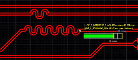
4. Utilize Serpentine Routing
Serpentine routing is a technique used to equalize the lengths of differential traces and maintain consistent impedance. By introducing deliberate meanders or serpentine patterns in the traces, any length mismatch between the positive and negative traces can be compensated for.
Serpentine routing offers the following advantages:
- Length Matching: By adding meanders to the shorter trace, the lengths of the positive and negative traces can be matched, ensuring balanced impedance.
- Impedance Control: The serpentine patterns can be designed to maintain the desired characteristic impedance by controlling the trace width and spacing.
- Flexibility: Serpentine routing allows for length matching even when the available routing space is limited or when dealing with complex PCB layouts.
Here’s an example of serpentine routing:
       ┌───────────────────────────────────────────────┐
       │                                               │
       │   Signal+   ───────────────────────────       │
       │             │                         │       │
       │             │                         │       │
       │             │                         │       │
       │   Signal-   └─────────────────────────┘       │
       │                                               │
       └───────────────────────────────────────────────┘

Simulation and Testing
To ensure that the differential trace impedance meets the desired specifications, simulation and testing are crucial steps in the design process.
Simulation Tools
There are several simulation tools available that can help in analyzing and optimizing differential trace impedance:
- Field Solvers: Field solvers, such as Ansys HFSS or Keysight ADS, use electromagnetic (EM) simulation to accurately model the behavior of differential traces. They take into account the trace geometry, PCB Stackup, and material properties to calculate the characteristic impedance and other parameters.
- Analytical Tools: Analytical tools, such as Polar Instruments’ Si8000m or Mentor Graphics’ HyperLynx, use mathematical equations and approximate models to estimate the differential trace impedance. While not as accurate as field solvers, they offer faster simulation times and are suitable for initial design exploration.
- PCB Design Software: Many PCB design software packages, such as Altium Designer or Cadence Allegro, include built-in tools for calculating and optimizing differential trace impedance. These tools often use a combination of analytical equations and EM simulation to provide impedance estimates.
Testing Methods
Once the PCB is fabricated, it is important to validate the differential trace impedance through testing. There are several methods commonly used for measuring impedance:
- Time Domain Reflectometry (TDR): TDR involves sending a fast-rising pulse down the differential traces and measuring the reflections caused by impedance discontinuities. By analyzing the reflected waveforms, the impedance profile along the traces can be determined.
- Vector Network Analyzer (VNA): A VNA measures the scattering parameters (S-parameters) of the differential traces over a range of frequencies. From the S-parameters, the characteristic impedance can be calculated. VNAs offer high accuracy and the ability to characterize the impedance across a wide frequency range.
- Impedance Test Coupons: Impedance test coupons are specially designed PCB structures that replicate the differential trace geometry and stackup. By measuring the impedance of these coupons using TDR or VNA, the actual impedance of the differential traces can be verified.

Best Practices for Differential Trace Impedance Control
To ensure consistent and reliable differential trace impedance, follow these best practices:
- Define Impedance Requirements: Clearly specify the target impedance for the differential traces based on the signaling standards and the desired performance.
- Choose Appropriate PCB Materials: Select PCB materials with stable dielectric constants and low loss tangents to minimize impedance variations and signal attenuation.
- Optimize Trace Geometry: Use appropriate trace widths, spacings, and thicknesses to achieve the desired impedance. Consult Impedance Calculators or simulation tools to determine the optimal geometry.
- Maintain Symmetry: Ensure that the differential traces are symmetrical and have equal lengths to maintain balanced impedance. Use serpentine routing or length matching techniques when necessary.
- Minimize Discontinuities: Avoid abrupt changes in trace width or direction. Use smooth bends and transitions to maintain consistent impedance.
- Provide Adequate Clearance: Ensure sufficient clearance between the differential traces and other traces or components to minimize coupling and impedance variations.
- Simulate and Test: Perform simulations to verify the impedance of the differential traces during the design phase. Conduct thorough testing and measurements on the fabricated PCB to validate the actual impedance.
- Document and Communicate: Clearly document the impedance requirements, design guidelines, and test results. Communicate this information to all stakeholders, including PCB fabricators and assembly partners, to ensure consistent implementation.

Frequently Asked Questions (FAQ)
- What is the importance of differential trace impedance in high-speed PCB design?
Differential trace impedance is crucial in high-speed PCB design because it directly impacts signal integrity and performance. Mismatched or inconsistent impedance can lead to reflections, signal distortions, and increased electromagnetic interference (EMI). By carefully controlling the differential trace impedance, designers can ensure reliable and error-free data transmission. - How does the absence of a reference plane affect differential trace impedance?
The absence of a reference plane can make it more challenging to maintain consistent differential trace impedance. Without a reference plane, the impedance of the differential traces becomes more sensitive to the presence of nearby traces and the PCB stackup. The lack of shielding provided by a reference plane also makes the traces more susceptible to EMI and coupling effects. - What are some common techniques for maintaining differential trace impedance without a reference plane?
Some common techniques for maintaining differential trace impedance without a reference plane include: - Carefully controlling the trace geometry, including trace width, spacing, and symmetry.
- Using a coplanar waveguide (CPW) structure, where ground traces accompany the differential traces on the same layer.
- Employing a differential microstrip structure, with the differential traces on the top layer and a ground plane on the layer beneath.
- Utilizing serpentine routing to equalize the lengths of differential traces and maintain consistent impedance.
- How can simulation tools assist in analyzing and optimizing differential trace impedance?
Simulation tools, such as field solvers and analytical tools, can help in analyzing and optimizing differential trace impedance by: - Accurately modeling the behavior of differential traces based on trace geometry, PCB stackup, and material properties.
- Calculating the characteristic impedance and other parameters to ensure they meet the desired specifications.
- Allowing designers to explore different design options and optimize the trace geometry for impedance control.
- Providing insights into potential impedance discontinuities and helping to identify areas for improvement.
- What are some best practices for ensuring consistent and reliable differential trace impedance?
Some best practices for ensuring consistent and reliable differential trace impedance include: - Clearly defining the impedance requirements based on the signaling standards and desired performance.
- Choosing appropriate PCB materials with stable dielectric constants and low loss tangents.
- Optimizing trace geometry, maintaining symmetry, and minimizing discontinuities.
- Providing adequate clearance between differential traces and other traces or components.
- Performing simulations and thorough testing to verify and validate the impedance.
- Documenting and communicating the impedance requirements, design guidelines, and test results to all stakeholders.
By understanding the challenges and employing the appropriate techniques and best practices, designers can effectively maintain differential trace impedance even in the absence of a reference plane, ensuring reliable and high-performance PCB designs.