

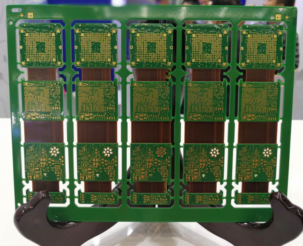
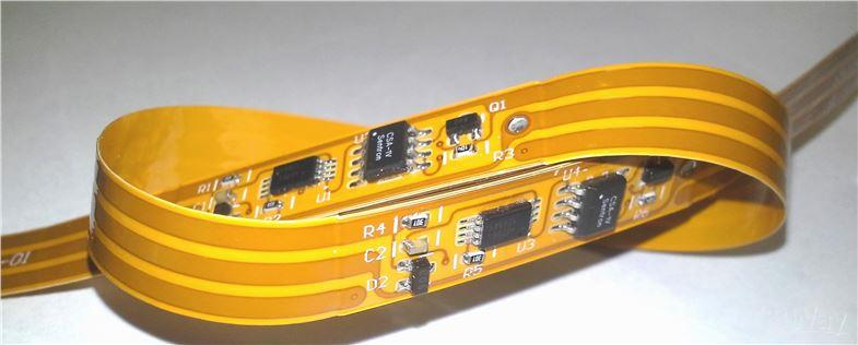
Flexible printed circuits (FPCs) are a crucial component in modern electronic devices. As products continue to get smaller and more portable, FPCs allow circuitry to bend and flex with the devices. Altium Designer provides powerful tools for designing flexible PCBs, including the Layer Stack Manager for configuring the layer stack.
Overview of Flexible PCBs
A flexible PCB is composed of a base insulating material, like polyimide, with conductive traces etched or printed on top. The lack of a rigid fiberglass substrate allows the PCB to bend and twist. Common applications include:
- Displays
- Wearable devices
- Medical devices
- Consumer electronics
Flexible PCBs provide many advantages:
- Ability to fit and flex inside small and irregular enclosures
- Dynamic flexing and repeated bending
- Lightweight and thin
- High density interconnects
The layer stack defines the layer structure of the PCB. For an FPC, the stackup includes a flexible dielectric base material, conductive copper layers, and coverlay/soldermask layers. The key is optimizing the stackup for the required application.
Altium Layer Stack Manager
Altium Designer’s Layer Stack Manager provides full control over the layer stack when designing flexible PCBs. The manager allows you to:
- Choose dielectric and copper foil materials
- Set dielectric thicknesses
- Configure laminate stacking sequence
- Define different stackups for rigid and flex sections
- Set layer colors
The Layer Stack Manager integrates with Altium’s PCB editor for a streamlined workflow. After defining the stackup, you can start routing traces on the appropriate signal layers. The software also handles complex tasks like length matching and differential pairs.
The Layer Stack Manager removes the manual work of planning out the layer structure. The intelligent PCB editor then reflects the stackup through color-coded layers, 3D views, and design rule checking.
Typical FPC Layer Stackup
While the layer stack can be configured in different ways, here is a typical 8-layer sequence:
- Coverlay/Soldermask
- Signal 1
- Signal 2
- Ground 1
- Ground 2
- Signal 3
- Signal 4
- Flex Dielectric
The thin dielectric is at the core, providing a flexible base. Signal traces are distributed through the cross-section on copper foils. Ground planes provide controlled impedance and shielding. Additional layers can be added for more complex designs.
Coverlay or soldermask flex layers help prevent oxidation and protect during assembly. Strategically placed openings in the soldermask provide connectivity.
Examples of Altium FPC Layer Stacks
To demonstrate Altium’s capabilities, here are some example flex layer stackups produced with the Layer Stack Manager:
4-Layer FPC
| Layer | Type | Thickness | Material | Color | Notes |
|---|---|---|---|---|---|
| Top Soldermask | Flex | 0.003mm | Liquid Photoimageable Soldermask | Green | Openings defined in layer |
| Signal 1 | Copper | 0.035mm | Rolled Annealed | Cyan | Bottom layer traces |
| Dielectric 1 | Flex | 0.025mm | Polyimide | Gray | Thin base material |
| Signal 2 | Copper | 0.035mm | Rolled Annealed | Yellow | Top layer traces |
- 4 total layers
- Single polyimide flexible dielectric core
- Soldermask opens selectively exposed
6-Layer Rigid-Flex
| Layer | Type | Thickness | Material | Color | Notes |
|---|---|---|---|---|---|
| Top Soldermask | Flex | 0.003mm | Liquid Photoimageable Soldermask | Green | Covers rigid portion |
| Signal 1 | Copper | 0.035mm | Rolled Annealed | Cyan | |
| Dielectric 1 | Flex | 0.05mm | Polyimide | Gray | Base flex dielectric |
| Signal 2 | Copper | 0.035mm | Rolled Annealed | Yellow | |
| Dielectric 2 | Rigid | 0.2mm | FR-4 | White | Adds rigidity in section |
| Signal 3 | Copper | 0.035mm | Rolled Annealed | Orange |
- Polyimide flex base
- FR-4 rigid section for stiffness
- Continuous soldermask layer
Best Practices for Optimized Layer Stacks
Here are some tips for getting the most out of Altium’s Layer Stack Manager when designing FPCs:
- Clearly define rigid vs. flex sections – Use dedicated stackups in each area
- Minimize dielectric layers – Allows thin and light circuits
- Balance layer distribution – Spread layers through cross-section
- Utilize plane layers – In internal layers for shielding
- Adjust dielectric tolerances – Compensate for flexing and vibration
- Add coverlay/soldermask – Prevents oxidation and damage
- Follow industry guidelines – IPC specifications give stackup advice
Frequently Asked Questions
Here are some common questions around flexible PCB layer stacks in Altium:
What are the minimum bend radius rules for FPCs?
The minimum bend radius depends on the stackup, especially the thickness. Typical FR-4 PCBs have a minimum bend radius around 10x the thickness. For flex PCBs, it can be 5x-7x the thickness. Follow manufacturer recommendations for the flex dielectric material used.
How do I handle shielding on outer layers of the FPC?
If shielding is required, include a grounded copper layer directly under the soldermask rather than leaving the dielectric exposed. An inner layer ground plane also provides shielding. Careful routing helps avoid noise coupling between traces.
What dielectrics are best suited for dynamic flex applications?
Polyimide films like DuPont’s Kapton provide excellent flexibility and durability for dynamic bending. These flex materials have high bend cycles before failure and maintain stable electrical and mechanical properties.
Why use a soldermask on flexible circuits?
The soldermask prevents oxidation and corrosion of the copper traces. It also insulates between traces to avoid shorting. Openings in predefined locations allow selective connections during component termination.
How can I reduce costs when designing flex layer stacks?
Stackup optimization is key. Minimize the number of layers and dielectric materials used. Consolidate plane layers when possible. Talk to your PCB manufacturer, as they may have recommendations to reduce costs. Consider standard materials rather than exotic flex substrates.
Conclusion
Flexible PCBs enable innovative and compact product designs. Altium Designer’s Layer Stack Manager provides the advanced tools needed to design optimized FPC layer stacks. Engineers can define flexible substrates, stackup sequence, and materials within an intelligent PCB design environment. Following best practices when architecting the flex board layer structure results in a quality PCB optimized for the target application.