

What are HDI PCBs?
High Density Interconnect (HDI) printed circuit boards are a type of PCB that incorporate higher wiring density per unit area compared to conventional PCBs. This is achieved through the use of finer lines and spaces (<100 μm), micro vias (<150 μm), and capture pads (<400 μm). HDI PCB technology enables miniaturization, improved electrical performance, and higher interconnect density for advanced electronics applications.
The main characteristics of HDI PCBs include:
– High wiring density (>120 in/in2)
– Fine pitch components
– Blind and buried vias
– Sequential lamination
– Laser-drilled microvias
HDI PCBs are used in a wide range of applications that require high performance, reliability, and compact form factors, such as:
– Smartphones and tablets
– Wearable devices
– Medical devices
– Automotive electronics
– Aerospace and defense systems
– High-speed networking equipment
– Supercomputers and data centers
Advantages of HDI PCBs
HDI PCB technology offers several key benefits over traditional PCB Designs:
- Miniaturization: HDI allows for smaller component sizes and higher I/O density, enabling more functionality to fit in compact device footprints. This is critical for mobile and wearable devices.
- Performance: With shorter signal paths and controlled impedance, HDI improves signal integrity, reduces crosstalk and EMI issues, and supports high-speed data transmission.
- Reliability: The use of microvias and stacked vias enhances thermal management and improves overall reliability by minimizing CTE mismatches between the PCB and components.
- Cost reduction: Although HDI boards have higher fabrication costs initially, they often lead to overall cost savings by eliminating the need for multiple interconnect layers and enabling higher manufacturing yields.
- Design flexibility: HDI stackups allow for creative routing solutions and 3D packaging techniques like package-on-package (PoP) and chip-scale packaging (CSP).

HDI PCB Design Considerations
Designing HDI PCBs requires careful planning and adherence to specific guidelines to ensure manufacturability, signal integrity, and reliability. Some key considerations include:
1. Material Selection
The choice of dielectric material is crucial for HDI PCBs due to the high wiring density and signal speeds involved. The material should have:
– Low dielectric constant (Dk) and dissipation factor (Df) for high-speed performance
– Good thermal stability and low CTE for reliability
– Laser drillability for microvia formation
– Smooth copper surface for fine pitch traces
Some commonly used HDI materials are:
| Material | Dk | Df | Tg (°C) | CTE (ppm/°C) |
|---|---|---|---|---|
| FR-4 | 4.4 | 0.02 | 130-140 | 14-16 |
| Megtron 6 | 3.3 | 0.004 | 210 | 10-12 |
| ALIVH-5 | 3.8 | 0.009 | 200 | 11-13 |
| I-Speed | 3.0 | 0.0035 | 200 | 10-15 |
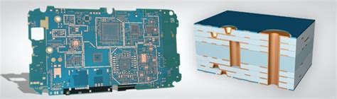
2. Layer Stackup Design
HDI PCBs often employ complex multilayer stackups with microvias to achieve high wiring density and signal integrity. The stackup design should consider:
– Number of signal, power, and ground layers
– Microvia span (stacked, staggered, or stacked-and-staggered)
– Controlled impedance requirements
– Shielding and isolation of sensitive signals
– Symmetric construction for warpage control
Here is an example 8-layer HDI stackup:
| Layer | Material | Thickness (μm) |
|---|---|---|
| Top | Copper | 17.5 |
| L1-L2 | Prepreg | 100 |
| L2 | Copper | 17.5 |
| L2-L3 | Core | 200 |
| L3 | Copper | 17.5 |
| L3-L4 | Prepreg | 100 |
| L4 | Copper | 17.5 |
| L4-L5 | Core | 400 |
| L5 | Copper | 17.5 |
| L5-L6 | Prepreg | 100 |
| L6 | Copper | 17.5 |
| L6-L7 | Core | 200 |
| L7 | Copper | 17.5 |
| L7-L8 | Prepreg | 100 |
| Bottom | Copper | 17.5 |
3. Microvia Design
Microvias are a key enabler for HDI PCBs, allowing for interconnections between layers without consuming valuable routing space. However, they also introduce design challenges and reliability concerns. Some guidelines for microvia design are:
- Limit microvia aspect ratio to 0.75:1 for reliability
- Use a minimum drill size of 75 μm for manufacturability
- Provide adequate capture pad size and clearance
- Avoid stacking more than two microvias to prevent barrel cracking
- Use IPC-4761 specifications for microvia formation and acceptance
4. High-Speed Design
HDI PCBs often carry high-speed digital signals that are susceptible to signal integrity issues like reflections, crosstalk, and EMI. To mitigate these problems, designers should:
- Use controlled impedance traces with proper terminations
- Match trace lengths for critical signals
- Provide adequate ground and power planes for current return paths
- Minimize via stubs and unterminated traces
- Implement differential pair routing for high-speed interfaces like PCIe or USB
- Follow high-speed design rules for spacing, coupling, and reference plane changes

HDI PCB Manufacturing Process
The manufacturing process for HDI PCBs is more complex and requires specialized equipment compared to conventional PCBs. The key steps involved are:
- Inner layer processing: The inner layers are patterned using standard photolithography and etching processes, similar to conventional PCBs.
- Lamination: The patterned inner layers are stacked with prepreg and copper foils, then laminated under high temperature and pressure to form a multilayer board.
- Drilling: Mechanical drilling is used to create through holes and blind vias, while laser drilling is employed for microvias. The laser type (CO2, UV, or YAG) depends on the material and via size.
- Desmear: A chemical or plasma desmear process is used to remove resin smear and debris from the drilled holes, ensuring a clean surface for copper plating.
- Electroless copper plating: A thin layer of copper is deposited on the hole walls and surface using an electroless plating process, providing electrical conductivity for subsequent electrolytic plating.
- Electrolytic copper plating: The board is electroplated with copper to the desired thickness, typically 20-25 μm for HDI PCBs.
- Outer layer processing: The outer layers are patterned using photolithography and etching, similar to the inner layers.
- Solder mask and surface finish: A solder mask is applied to protect the copper traces, and a surface finish (ENIG, OSP, or Immersion Ag) is applied to the exposed pads for solderability.
- Electrical test: The finished HDI PCB undergoes electrical testing, such as automated optical inspection (AOI), Flying Probe test, or in-circuit test (ICT) to verify its functionality and compliance with specifications.

HDI PCB Cost Drivers
While HDI PCBs offer many technical advantages, they also come with higher fabrication costs compared to conventional PCBs. The main cost drivers for HDI PCBs are:
- Material: HDI-grade laminates and prepregs are more expensive than standard FR-4 due to their enhanced properties and tighter tolerances.
- Layer count: The number of layers directly affects the HDI PCB cost, as each additional layer requires more processing steps and materials.
- Microvia density: A higher number of microvias per board increases the fabrication cost, as it requires more laser drilling time and specialized equipment.
- Aspect ratio: Microvias with higher aspect ratios (>0.75:1) are more challenging to manufacture reliably, thus increasing the cost.
- Surface finish: Advanced surface finishes like ENIG or Immersion Ag are more expensive than standard HASL due to the precious metals used.
- Testing: Comprehensive electrical testing, such as flying probe or boundary scan, adds to the overall cost but is necessary to ensure HDI PCB reliability.
Despite the higher initial costs, HDI PCBs can provide long-term cost savings by enabling miniaturization, higher yields, and reduced assembly complexity. A cost-benefit analysis should be conducted to determine the viability of HDI for a given application.
FAQ
1. What is the difference between HDI and standard PCBs?
HDI PCBs have higher wiring density (>120 in/in2), finer pitch components, and use microvias for layer interconnections, while standard PCBs have lower wiring density (<100 in/in2), larger components, and use conventional through-hole vias.
2. What are the benefits of using HDI PCBs?
The main benefits of HDI PCBs are miniaturization, improved electrical performance, higher reliability, cost reduction, and design flexibility compared to conventional PCBs.
3. What materials are commonly used for HDI PCBs?
Common HDI PCB materials include high-performance laminates like Megtron 6, ALIVH-5, and I-Speed, which offer low dielectric constant, low loss, and good thermal stability compared to standard FR-4.
4. What is the minimum microvia size achievable with HDI technology?
The minimum microvia size for HDI PCBs is typically 75 μm in diameter, with an aspect ratio of 0.75:1 for reliable fabrication.
5. Are HDI PCBs more expensive than standard PCBs?
Yes, HDI PCBs have higher fabrication costs due to the specialized materials, equipment, and processes involved. However, they can provide overall cost savings through miniaturization, higher yields, and reduced assembly complexity.
Conclusion
High Density Interconnect PCBs are a key enabling technology for the growing demand for miniaturization, performance, and reliability in modern electronics. By leveraging advanced materials, design techniques, and manufacturing processes, HDI PCBs offer a wide range of benefits over conventional PCBs, including higher wiring density, improved signal integrity, and greater design flexibility.
However, designing and manufacturing HDI PCBs also present unique challenges and considerations, such as material selection, layer stackup design, microvia optimization, high-speed signal routing, and cost management. A thorough understanding of HDI design guidelines, manufacturing processes, and cost drivers is essential for successful implementation.
As electronic devices continue to push the boundaries of functionality and form factor, HDI PCB technology will play an increasingly critical role in enabling the next generation of smartphones, wearables, medical devices, automotive electronics, and high-performance computing systems. By staying up-to-date with the latest advancements and best practices in HDI PCB design and manufacturing, engineers and product developers can unlock new possibilities for innovation and differentiation in their respective markets.