

Introduction
Printed circuit boards (PCBs) provide the foundation for almost all modern electronics. PCBs allow electrical components to be mechanically supported and electronically connected. Traditionally, PCBs have been made from rigid laminate materials like FR-4. However, flexible PCBs (flex PCBs) have become increasingly popular in recent years due to their ability to bend and flex. Combining rigid and flex PCB technologies allows for more compact and ergonomic product designs. This article provides an overview of rigid and flex PCBs, their design considerations, and manufacturing processes.
Rigid PCBs
What are Rigid PCBs?
Rigid PCBs are made from stiff laminate materials that do not bend or flex during use. The most common material used is FR-4, a glass reinforced epoxy laminate. Other materials like polyimide and ceramic substrates are also used for specialized high frequency or high temperature applications. Rigid PCBs provide structural support for mounted components while insulating and connecting traces between them.
Rigid PCB Design Considerations
Several factors need to be considered when designing rigid PCBs:
- Board Size – The dimensions of the board are usually dictated by the product enclosure but optimize for efficient panel utilization.
- Layer Stackup – Determine number of copper layers and dielectric materials needed. More layers provide higher routing density.
- High Speed Traces – Control impedance through trace dimensions and routing planes. Avoid 90° turns.
- Component Placement – Position components for efficient routing and minimize trace lengths. Consider grouping by type.
- Thermal Management – Ensure adequate thermal dissipation through board layers and copper fills. Add thermal vias if needed.
- EMI/EMC – Include proper grounding, filtering, and shielding in the design to reduce unwanted emissions and susceptibility.
Rigid PCB Manufacturing Process
Rigid PCB manufacturing involves many steps to produce the bare board:
- Prototyping – Initial short run boards are fabricated to test design and functionality.
- Fabrication Data Preparation – CAD data is processed into manufacturing files used for phototools or direct imaging.
- Imaging – Desired circuit pattern is transferred to photoresist on copper clad laminate via lithographic process.
- Etching – Exposed copper is etched away leaving only intended copper traces.
- Lamination – Multilayer boards are constructed by laminating etched inner layers together under heat and pressure.
- Drilling – Holes are mechanically drilled for component leads and vias.
- Plating – Walls of drilled holes are plated with copper to provide conductivity between layers.
- Solder mask – Epoxy layer is applied to protect exposed copper traces.
- Silkscreen – Printed markings identify components, connections, and board details.
- Final Finishing – Boards are routed, trimmed, inspected, and electrically tested.
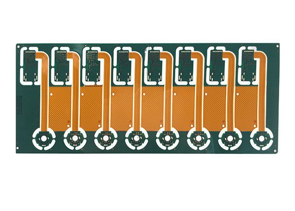
Flex PCBs
What are Flex PCBs?
Flex PCBs use a flexible dielectric base material that allows the board to bend and twist. Common flex circuit materials include polyimide, polyester, and PEEK. Flex PCBs were originally designed for military aerospace applications but now used in various consumer products. Flex circuits provide unique mechanical and electrical properties.
Benefits of Using Flex PCBs
Flex PCBs offer several advantages compared to rigid boards:
- Flexible – Can be dynamically contorted and shaped to application.
- Thin and Lightweight – Extremely thin flexible materials down to 1 mil. Save space and weight.
- Highly Customizable – Flexible circuits can be sculpted and formed into unique shapes.
- Durable – Withstand vibration, shock, and flexing stresses.
- High Density – Small traces and spacing allows higher connection density.
Flex PCB Design Considerations
Designing flex PCBs have additional considerations:
- Minimum Bend Radius – Avoid overflexing and damaging flex materials.
- Layer Stackup – Use thinner, flexible dielectrics for inner layers. Control overall thickness.
- Component Placement – Position parts for reliability across bends and folds.
- Stiffener Integration – Strategically locate rigid sections for mounting stability.
- ESD Protection – Polyimide does not dissipate charges well. Add grounding features.
- Thermal Management – Flexible materials conduct heat poorly. Use thermal adhesives or sinks.
Flex PCB Manufacturing Process
Flex PCB fabrication has similarities to rigid PCBs but also important differences:
- Design and Prototyping – Products must be modeled in flat, flexed, and ruggedized states.
- Imaging – Photolithography transfers circuit patterns onto rolled flex materials.
- Etching – Unwanted copper removed to isolate circuit traces.
- Die Cutting – Flex circuits are precision cut to specified outlines.
- Layer Bonding – Adhesive films bond multiple layers together into flex assemblies.
- Component Assembly – SMT, PTH, or conductive epoxies attach components.
- Encapsulation – Entire assembly optionally potted for environmental protection.
- Sculpting – Flex circuits are shaped into 3D configurations as needed.
- Testing and Inspection – 100% electrical testing and visual inspection.
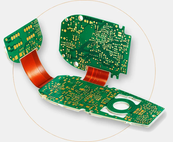
Rigid-Flex PCBs
What are Rigid-Flex PCBs?
Rigid-flex PCBs integrate rigid and flex materials into one circuit solution. They contain rigid sections for component mounting along with flexible interconnects between sections. Varying the proportion of rigid and flex allows optimization of mechanical and electrical properties. Rigid-flex is ideal for complex applications like foldable mobile devices.
Benefits of Rigid-Flex PCBs
Rigid-flex PCBs offer the combined advantages of both technologies:
- Component Mounting – Rigid areas for attaching ICs, connectors, and other components.
- Dynamic Flexing – Flexible bend areas for movement and vibration.
- Layer Interconnections – Continuous connectivity between different rigid segments.
- Compact Stackup – Thin profile by embedding components within layers.
- Weight Reduction – Eliminate wires and connectors between PCBs.
Rigid-Flex Design Considerations
Rigid-flex PCB require careful design planning:
- Rigid-Flex Transition – Manage differences in material properties with teardrop shapes and back cuts.
- Layer Configuration – Determine which layers route continuously along flex areas.
- Flexible Bend Radii – Ensure radii do not overstress flex layers.
- Component Placement – Position parts optimally across rigid and flex areas.
- Fold and Stacking – Account for order, spacing, and stacking of folds.
- Board Outline – Profile rigid sections for efficient panel utilization.
Rigid-Flex Manufacturing Process
Rigid-flex PCB fabrication combines processes of rigid and flex PCBs:
- Design and Prototyping – Develop mechanical models of flat, folded, and flexed states.
- Fabrication Data – Separate rigid and flex data sets prepared.
- Rigid Lamination – Fabricate core rigid layers similarly to rigid PCB.
- Flex Patterning – Image and etch flex layers separately.
- Layer Alignment – Align and laminate rigid and flex layers together.
- Drilling and Plating – Drill holes through rigid and flex sections.
- Component Assembly – Populate components on rigid sections.
- Sculpting – Shape flex areas into designed 3D configurations.
- Testing – Functionally test PCB electrically and mechanically.
Comparing Rigid, Flex, and Rigid-Flex PCBs
| PCB Type | Rigid PCB | Flex PCB | Rigid-Flex PCB |
|---|---|---|---|
| Composition | Rigid FR4 | Flexible polymer | Combination |
| Key Characteristics | Structural stability | Dynamic flexion | Integrates rigid and flex |
| Typical Thickness | 1.6 mm | 25-500 μm | Varies |
| Layers | Up to 30+ | 1-12 | 10-20+ |
| Minimum Trace | 6 mil | 2 mil | 4 mil |
| Popular Uses | High density interconnect | Wearables, medical | Foldable devices |
| Relative Cost | Low | Moderate | High |
Conclusion
Rigid, flex, and rigid-flex PCB technologies each offer unique advantages. Rigid PCBs provide stability for high density components. Flex circuits allow dynamic routing and compactness through extreme flexibility. Rigid-flex combines both abilities into a single solution for complex applications. Careful design consideration is required to leverage the benefits of each technology. Working with an experienced PCB manufacturer optimizes the fabrication process and end product quality.
Frequently Asked Questions
What are some examples of rigid PCB applications?
Some common applications of rigid PCBs include computers, servers, telecommunications infrastructure, LED lighting, automotive electronics, industrial control systems, and medical equipment. Rigid boards are ideal for densely packed, high speed digital circuits.
What materials are used to make flex PCBs?
The most common materials used for flex PCB dielectric layers are polyimide, polyester, polyethylene naphthalate, and fluorinated ethylene propylene. Polyimide provides the best electrical performance at a higher cost.
How are components assembled on flex PCBs?
For flex PCB assemblies, surface mount packages are most often used. Smaller components can be attached with conductive epoxy. Stiffeners support and strengthen soldered sections. Automated pick and place equipment assemble components onto flex materials.
How many bends can a flex PCB withstand?
The flex life depends on trace thickness, material type, bend radius, and cycles. Typical flex PCBs can withstand 100,000 to 1 million+ dynamic bend cycles for well-designed small radii bends. Flex circuits can be folded and unfolded reliably as well.
Should traces be routed on one or both sides of a flex PCB?
For dynamic flex applications with tight bend radii, routing traces on a single side is recommended. Stacking traces on both sides increases likelihood of fracturing due to differences in elongation and compression.